CY3220LINBUS-RD Cypress Semiconductor Corp, CY3220LINBUS-RD Datasheet
CY3220LINBUS-RD
Specifications of CY3220LINBUS-RD


Related parts for CY3220LINBUS-RD


CY3220LINBUS-RD Summary of contents
Page 1
PSoC CY8C20x34 TRM ® PSoC CY8C27x43, CY8C27x43E, LIN Bus 2.0 PSoC Reference Design. Revision ** San Jose, CA 95134-1709 Phone (USA): 800.858.1810 Phone (Intnl.): 408.943.2600 CY8C29x66, CY8C21x34 Cypress Semiconductor 198 Champion Court http://www.cypress.com ...
Page 2
... Copyright © 2006 Cypress Semiconductor Corporation. All rights reserved. Cypress, the Cypress logo, and PSoC® are registered trademarks and PSoC Designer™, Programmable System-on-Chip™, and PSoC Express™ are trademarks of Cypress Semiconductor Corporation (Cypress). All other trademarks or registered trademarks referenced herein are the property of their respective owners. ...
Page 3
Contents 1.1 LIN Bus 2.0 Demonstration Kit Description .......................................................................................5 1.1.1 Introduction ..............................................................................................................5 1.2 Kit Contents ...............................................................................................................................5 1.3 Getting Started ...........................................................................................................................5 1.4 LIN Bus Demonstration ..............................................................................................................6 1.5 Master Node Port Pin Usage .....................................................................................................9 1.6 Slave 1 Port Pin Usage ..............................................................................................................9 1.7 ...
Page 4
Contents 3.4 Source Code Files ................................................................................................................... 18 3.5 Header Files ............................................................................................................................ 18 3.6 Creating a Project Using the Design IP ................................................................................... 18 3.6.1 Importing the Design ............................................................................................. 18 3.6.2 Configuring Global Resources............................................................................... 19 3.6.3 Configuring GPIO .................................................................................................. 19 3.6.4 Routing ...
Page 5
Frame Definition.....................................................................................................37 4.6.7 Response_Error Bit Definition................................................................................37 4.6.8 Node Information ...................................................................................................37 4.6.9 Adding the Main Application ..................................................................................37 4.6.10 Special Features ....................................................................................................38 4.6.10.1 4.6.10.2 4.6.10.3 4.7 LIN 2.0 Slave Design API ........................................................................................................39 4.8 Time Study ...............................................................................................................................40 4.8.1 ISR and Function ...
Page 6
Contents 4 LIN Bus 2.0 Reference Design ...
Page 7
LIN Bus 2.0 Kit 1.1 LIN Bus 2.0 Demonstration Kit Description 1.1.1 Introduction The LIN Bus Demonstration Kit demonstrates the ability of the PSoC® Programmable System-on-Chip™ to implement LIN bus, Local Interconnect Network, standard protocol. The LIN bus was ...
Page 8
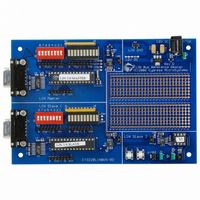
LIN Bus 2.0 Kit Master Serial Port Slave 1 Figure 1-1. LIN Bus Demonstration Board The master node and slave 1 are both implemented in a 28- pin part, CY8C27443-24PXI. Slave 2 is implemented in an 8-pin part, CY8C27143-24PXI. ...
Page 9
LIN Bus 2.0 Reference Design SW2 U7 SW1 Figure 1-2. Layout of Node-Specific Switches and LEDs Periodically, the master node sends its switch state informa- tion to slave 1 and then polls both slaves for their switch state information. In ...
Page 10
LIN Bus 2.0 Kit Figure 1-3. Switch-to-LED Control Relationship The master node performs the following operations. ■ Initializes the LIN communication. ■ Calls the node configuration function to configure slave 1 and slave 2 nodes. ■ Initializes the Schedule ...
Page 11
LIN Bus 2.0 Reference Design 1.5 Master Node Port Pin Usage The pin usage for the LIN bus PSoC master node is as fol- lows: Table 1-1. Port 0 – Pins Connect to User-Accessible Header Row 0 Not used 1 ...
Page 12
LIN Bus 2.0 Kit 1.7 Slave 2 Port Pin Usage The section details the pin usage for the LIN bus PSoC slave 2: Table 1-7. Port 0 – Pins 2 Push button controls master, Port1_3 LED 4 LIN bus ...
Page 13
System Architecture 2.1 Overview The LIN bus, Local Interconnect Network asynchro- nous, 1 wire, single master, multiple slave network most commonly used in automobile networks. 2.2 Features of the PSoC LIN Bus 2.0 Design ■ ...
Page 14
System Architecture Figure 2-2. Structure of a Byte Field 2.3.2 Break Field The break symbol is used to signal the beginning of a new frame the only field that does not comply with Figure ...
Page 15
LIN Bus 2.0 Reference Design frames in the Schedule table have been transmitted, the next cycle starts again from the first frame of the table. The LIN 2.0 API has many functions to manage the Sched- ule table. It has ...
Page 16
System Architecture 14 Cypress Semiconductor – Rev. ** LIN Bus 2.0 Reference Design October 25, 2006 ...
Page 17
Master Design IP 3.1 Software Architecture 3.1.1 Overview The software architecture maximizes interrupt processing to minimize the processing overhead on the end application. All message processing through configurations is performed at the interrupt level. Each stage is designed as ...
Page 18
Master Design IP 3.1.3 Timing and Interrupts Automotive applications are often real-time driven result, the LIN driver only uses interrupts with no active loop or blocking functions. Overhead measurements made on a LIN bus with messages transferred ...
Page 19
LIN Bus 2.0 Reference Design 3.3 Firmware 3.3.1 Overview The initiation of a frame is done by the l_sch_tick function. This function first reads the Schedule table and loads the frame parameters of the frame to transmit. It then loads ...
Page 20
Master Design IP 3.3.5.3 Data Reception Configuration In the Data Reception Configuration, the bit time counter is configured to generate an interrupt every five bit times. Inside this ISR, a timeout counter is decremented by five. This timeout counter ...
Page 21
LIN Bus 2.0 Reference Design 7. The “Resolve name conflicts” window lists functions in the imported design that have the same name as func- tions in the existing project. When there is a name con- flict, clicking the “Auto Resolve” ...
Page 22
Master Design IP 8. Select Row_1_Input_x (step 7) as the input to the RX8 User Module. 9. Switch to the base configuration. 10. Make the connection from Row_1_Output_x net to the Global bus as used by the Data Transmission ...
Page 23
LIN Bus 2.0 Reference Design A. Checksum Type: This entry defines the checksum type used for the particular frame. There are two types of checksums, CSUM_CLASSIC and CSUM_EXTENDED. CSUM_CLASSIC is used for frames that belong to LIN slaves of version ...
Page 24
Master Design IP _MasterRequest: MasterRequest: db CSUM_CLASSIC ; Checksum Type Data count db abDiagBuffer ; Buffer address db MASTER_TO_SLAVE ; Direction db 0x3C ; ID _SlaveResponse: SlaveResponse: db CSUM_CLASSIC ; Checksum Type Data ...
Page 25
LIN Bus 2.0 Reference Design 3.6.11.2 An Example Schedule Table Here is an example Schedule table. The name of the table is Schedule1. This table has Frame1, Frame2, Frame3 and Frame4 (which are defined in the SignalTable.asm file) in the ...
Page 26
Master Design IP from this function. If the dominant state is less than 250 µ the state does not become recessive for more than 5 ms, the processor is put to sleep again. The pro- cessor can ...
Page 27
LIN Bus 2.0 Reference Design // Code to update the Frame5 buffer with the signal l_sporadic_frame_queue |= 0x04; } Only the bits corresponding to the frames in the Sporadic Frame table are set by the main function. 3.7 Master Design ...
Page 28
Master Design IP Example: For example, to write two bytes to Frame1 from the first byte of the buffer from another buffer called Temp- Buffer, use this code: l_bytes_wr(Frame1 TempBuffer); Note that the first byte of the ...
Page 29
LIN Bus 2.0 Reference Design Description: Clears the LIN ready flag. Parameters: None. Returns: None. LinMaster_SetReadyFlag C Prototype: void LinMaster_ClrReadyFlag (void); Description: Sets the LIN ready flag. This function is called inside the schedule timer’s ISR when a frame slot ...
Page 30
Master Design IP actually send the command, point the l_sch_set function to a master request frame and call the l_sch_tick function. ld_read_by_id C Prototype: void ld_read_by_id(l_u8 NAD, l_u16 supplier_id, l_u16 function_id, char* data); Description: This call requests the node ...
Page 31
LIN Bus 2.0 Reference Design The overall CPU overhead for a frame is calculated by add- ing all the time components for a frame and then finding the fraction of the total frame time. Remember, this method only gives the ...
Page 32
Master Design IP 30 Cypress Semiconductor – Rev. ** LIN Bus 2.0 Reference Design October 25, 2006 ...
Page 33
Slave Design IP 4.1 Software Architecture 4.1.1 Overview The software architecture maximizes interrupt processing to minimize the processing overhead on the end application. All processing of the current message using the configura- tions is performed at the interrupt level. ...
Page 34
Slave Design IP all slaves are required to monitor the bus at all times in prep- aration for the next message. 4.2 Device Configuration The LIN slave design has two configurations, the Synchro Reception Configuration and the Data Reception ...
Page 35
LIN Bus 2.0 Reference Design and backed up. The state machine is updated as “Wait For Falling Edge 1.” E. Wait For Falling Edge 1: When the first falling edge of the synch byte is detected, this state is entered. ...
Page 36
Slave Design IP the Synchro Reception Configuration is loaded to receive the next frame. ■ Waiting for Frame Completion: If, in the first step of decoding the protected ID found that the ID is not present in ...
Page 37
LIN Bus 2.0 Reference Design 4.6 Using the Design IP Follow these steps to create a LIN slave node using the Design IP. 4.6.1 Importing the Design There are two possible ways to import the design. One is to create ...
Page 38
Slave Design IP regardless of which configuration is active, the GPIO state of your main application is maintained. When you complete this process, the TX and RX pins configuration looks like the information in this table: Table 4-1. TX ...
Page 39
LIN Bus 2.0 Reference Design 4.6.6 Frame Definition You now define the frames. There are two tables in this file. One is the MESSAGE_ID_TABLE and the other is the ID_TABLE. Type the message ID list in the MESSAGE_ID table. Type ...
Page 40
Slave Design IP ing an application using PSoC Designer. Place the user modules in the base configuration, finish the routing, and generate application. In the main.c file, follow these steps to properly start the LIN firmware and to update ...
Page 41
LIN Bus 2.0 Reference Design SLAVE_TO_MASTER constant EVENT_TRIGGERED constant. Here is an example. _Frame3: Frame3: db 0xFF db SLAVE_TO_MASTER | EVENT_TRIGGERED db BufferFrame3 db 1 Once a frame is declared as event triggered and the frame is due, the program ...
Page 42
Slave Design IP l_signal_handle: Name of the frame to which bytes have to be written. start: The offset from where the bytes have to be written. count: Number of counts to be written. data: Buffer from which the data ...
Page 43
LIN Bus 2.0 Reference Design Table 4-6. TxInterrupt Sl. No. Stage 1 When a byte has been sent 166 2 When last byte has been sent 130 Table 4-7. TxBitTimerInterrupt Sl. No. Stage 1 All bytes transmitted 1200 Table 4-8. ...
Page 44
Slave Design IP 42 Cypress Semiconductor – Rev. ** LIN Bus 2.0 Reference Design October 25, 2006 ...
Page 45
Demonstration Projects 5.1 Introduction The LIN reference design board comes with three PsoC devices: ■ Master ■ Slave 1 ■ Slave 2 The master and slave 1 are implemented with 28-pin CY8C27443-PXI devices and slave 2 is implemented with ...
Page 46
Demonstration Projects 5.2.2 Example LDF LIN Description File Example /*******************************************/ /* /* Description: Example LIN Description /* Project: Lin20example /* Network: LIN_20 /* /* *******************************************/ LIN_description_file; LIN_protocol_version = "2.0"; LIN_language_version = "2.0"; LIN_speed = 19.2 kbps; Nodes { master ...
Page 47
LIN Bus 2.0 Reference Design SlaveRespB4:8,0; SlaveRespB5:8,0; SlaveRespB6:8,0; SlaveRespB7:8,0; } dynamic_frames {52} Frames { VL1_CEM_Frm1 : 48, CEM, 8 Switch1CEM, 0; Switch2CEM, 8; Switch3CEM, 16; Switch4CEM, 24; Switch5CEM, 32; Switch6CEM, 40; Switch7CEM, 48; Switch8CEM, 56; } VL1_CEM_Frm2 : 5, CEM, ...
Page 48
Demonstration Projects } SlaveResp //pub: any slave SlaveRespB0, 0; SlaveRespB1, 8; SlaveRespB2, 16; SlaveRespB3, 24; SlaveRespB4, 32; SlaveRespB5, 40; SlaveRespB6, 48; SlaveRespB7, 56 Node_attributes{ DIA { LIN_protocol = "2.0"; configured_NAD = 0x02; product_id = 0x1234, ...
Page 49
LIN Bus 2.0 Reference Design 5.3 Example Project for Master (CEM) 5.3.1 Description The master does the following: 1. Initialize the hardware and LIN core. 2. Configure the nodes in the network using the node configuration functions. 3. Initialize the ...
Page 50
Demonstration Projects NextTask = l_sch_tick(); } // Check if Frame1 has completed succesfully if(BufferFrame1[0] & bfLAST_TRANSACTION_OK Clear the bfLAST_TRANSACTION_OK flag BufferFrame1[0] &= ~bfLAST_TRANSACTION_OK; // Update the signals in Frame1 UpdateFrame1(); // Transmit the Master switch status on ...
Page 51
LIN Bus 2.0 Reference Design // If Bit 0 of second byte is 1, then switch On LED5 if(TempBuffer[1] & 0x01) { PRT1DR &= ~0x08; Transmitter_CPutString(" Else switch it off else { PRT1DR |= 0x08; Transmitter_CPutString("OFF "); } ...
Page 52
Demonstration Projects if(BufferFrame4[1] & Temp) Transmitter_CPutString("ON else Transmitter_CPutString("OFF "); Temp >> Transmitter_PutCRLF(); Transmitter_PutCRLF(); } } } void UpdateFrame1(void) { BYTE i; BYTE x; // Load up the 8 byte message with the status of DIP Switchs S2. ...
Page 53
LIN Bus 2.0 Reference Design do { bError = ConfigureNode(1, 0x1234, 0x1003, 0x32); Retries++; } while((bError == 1) && (Retries < 2)); // Configure Message 0x1001 of DIA Retries = bError = ConfigureNode(2, 0x1234, 0x1001, 0x80); Retries++; ...
Page 54
Demonstration Projects 5.4 Example Project for Slave 1 (CPM) 5.4.1 Description Following are the functions performed by slave 1: 1. Initialize the hardware resources for resistance measurement, DIP switches and the LIN core. 2. Clear the Response_Error bit. 3. ...
Page 55
LIN Bus 2.0 Reference Design // Start the ADC and Start Conversion ADC_Start(ADC_MEDPOWER); ADC_StartAD(); // Enable Global Interrupts M8C_EnableGInt; // Infinite loop while( Read the LIN status TransferStatus = (char)l_ifc_read_status(); // Check if Frame1 has been successfully received. ...
Page 56
Demonstration Projects if(bResponseError) BufferFrame2[2] |= RESPONSE_ERROR_MASK; // Process Frame3. This frame is an Event triggered one. // has been any change in value on the switches connected to Port2. // there is a change, update the Frame3 buffer with ...
Page 57
LIN Bus 2.0 Reference Design // Enable Global Interrupts M8C_EnableGInt; // Infinite loop // Inside the while Loop, following operations are performed l_ifc_read_status is called to check the status of the LIN core Frame1 data is ...
Page 58
Demonstration Projects 56 Cypress Semiconductor – Rev. ** LIN Bus 2.0 Reference Design October 25, 2006 ...
Page 59
Board Schematics 6.1 Schematics 6.1.1 Power Supply October 25, 2006 Cypress Semiconductor – Rev ...
Page 60
Board Schematics 6.1.2 Master 56 Cypress Semiconductor – Rev. ** LIN Bus 2.0 Reference Design October 25, 2006 ...
Page 61
LIN Bus 2.0 Reference Design 6.1.3 Slave 1 October 25, 2006 Cypress Semiconductor – Rev Board Schematics 57 ...
Page 62
Board Schematics 6.1.4 Slave 2 58 Cypress Semiconductor – Rev. ** LIN Bus 2.0 Reference Design October 25, 2006 ...
Page 63
Board Bill of Materials October 25, 2006 Cypress Semiconductor – Rev ...
Page 64
Board Bill of Materials 60 Cypress Semiconductor – Rev. ** LIN Bus 2.0 Reference Design October 25, 2006 ...