CY3220LINBUS-RD Cypress Semiconductor Corp, CY3220LINBUS-RD Datasheet - Page 19
CY3220LINBUS-RD
Manufacturer Part Number
CY3220LINBUS-RD
Description
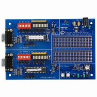
KIT REF DESIGN LIN BUS
Manufacturer
Cypress Semiconductor Corp
Series
PSoC®r
Datasheet
1.CY3220LINBUS-RD.pdf
(64 pages)
Specifications of CY3220LINBUS-RD
Main Purpose
Interface, LIN
Embedded
Yes, MCU, 8-Bit
Utilized Ic / Part
CY8C27143, CY8C27443
Processor To Be Evaluated
CY8C27143-24PXI and CY8C27443-24PXI
Interface Type
RS-232
Lead Free Status / RoHS Status
Contains lead / RoHS non-compliant
Lead Free Status / RoHS Status
Lead free / RoHS Compliant, Contains lead / RoHS non-compliant
Other names
428-1926


LIN Bus 2.0 Reference Design
3.3
3.3.1
The initiation of a frame is done by the l_sch_tick function.
This function first reads the Schedule table and loads the
frame parameters of the frame to transmit. It then loads the
Synchro Break Configuration and starts the synchro break
timer. This timer is configured to generate a dominant state
of 13 bit times and a recessive (logic high level on the bus)
state of one bit time. On the terminal count interrupt of this
timer, the Data Transmission Configuration is loaded and
the synch byte of 0x55 is transmitted. The protected identi-
fier
MASTER_TO_SLAVE, all data bytes are transmitted one by
one with the checksum as the last byte. If the transfer type is
not MASTER_TO_SLAVE, then the Data Reception Config-
uration is loaded and the response from the slave is
received. Data is processed after all bytes are received.
Once the l_sch_tick function loads the Synchro Break Con-
figuration and starts the synchro break timer, the rest of the
frame is processed in the background, inside ISRs. More
about the ISRs will be explained in the following sections.
This enables the main function to run in the foreground.
There are four different interrupts processed inside the LIN
master. One or more of these interrupts may be active
depending upon the active state. The code inside each of
these ISRs is well commented so that it is very easy to
understand the operation.
3.3.2
The l_sch_tick function loads the Synchro Break Configura-
tion and starts the synchro break counter. The synch
counter clock is from the baud rate clock generator, which
runs at eight times the bit rate. The period of the synch
counter is set to 111. This is equal to 14 bit times. The com-
pare value of the counter is set to eight, which is equal to
one bit time. So the output of the counter remains low for 13
bit times and high for one bit time. At the terminal count, the
synchro break counter generates an interrupt. The Data
Transmission Configuration is loaded inside this ISR. 0x55
is then placed on the TX buffer to generate the synch field.
The rest of the frame is continued from the TX interrupt.
3.3.3
Inside the TX ISR, the program checks if this is the first
interrupt. If this is the first interrupt, 0x55 was placed in the
TX shift register and the buffer is empty. The bit time counter
is started and its interrupt enabled. This counter’s interrupt is
used to check for bit errors. The bNbDataToSend variable is
then checked. If this variable equals zero, no more bytes are
sent and the bfLAST_BYTE_SENT flag is set. The comple-
tion of the frame takes place inside the Bit_time_counter’s
ISR. If the bNbDataToSend is not zero, then the next byte
sent is transferred to the TX buffer. Then the bNbData-
ToSend variable is decremented by one before exiting the
ISR.
October 25, 2006
is
Firmware
transmitted
Overview
Synchro Break Interrupt
TX Interrupt
next.
If
the
Cypress Semiconductor – Rev. **
transfer
is
3.3.4
If a response is expected from the slave, the Data Reception
Configuration
Bit_time_counter’s ISR for the Data Transmission Configu-
ration. When a byte is received from the slave, this interrupt
is generated. Inside the interrupt, the received data is placed
on a buffer in the RAM. The bNbDataToReceive variable is
decremented and checked if zero. If it is not zero, the ISR is
exited. If this value becomes zero, it means that all the bytes
were received and the Synchro Break Configuration is
loaded to allow for the next frame initiation. Then the
bfDATA_TO_COPY flag is checked. This flag is set if this is
a SLAVE_TO_MASTER transaction and is not set if this is a
SLAVE_TO_SLAVE transaction. For a SLAVE_TO_SLAVE
transaction, the master has nothing to do with the received
data so the data is discarded. For a SLAVE_TO_MASTER
transaction, the checksum of the received data is verified. If
the checksum is valid, the received data is transferred to the
corresponding frame buffer. The checksum of the data bytes
is compared with the last byte of the frame, which is the
checksum transmitted by the slave. If they are identical, the
data is valid. If the data is a slave’s response to a master’s
diagnostics request, the received data is processed for the
RSID, error code etc. of the slave response. Details of RSID
may be found in the LIN 2.0 specifications.
3.3.5
The bit time interrupt is used in all the configurations.
3.3.5.1
In the Synchro Break Configuration, the bit time counter
generates an interrupt every bit time. Inside the ISR, the TX
and RX pins are compared to check if there is a bit error. If a
bit error is found, the frame is aborted and the Synchro
Break Configuration is reloaded. Also, when the TX state is
sensed as logic high, the TX pin is disconnected from the
global bus and made StdCPU and the TX pin’s state is made
logic high. This is done to prevent the counter output from
becoming logic low upon terminal count before it is stopped
inside the synchro break ISR. This unwanted low transition
could be taken as the falling edge of the synch byte by the
slaves connected to the cluster and may lead to communi-
cation errors.
3.3.5.2
In the Data Transmission Configuration, the bit time interrupt
is used to compare the TX and RX pins. The number of bits
compared is tracked by the bNbBitsAnalyzed variable. This
variable is initially set to 10, including the start and stop bits
of a byte. Whenever this variable becomes zero, a byte is
analyzed and the bfLAST_BYTE_TRANSMITTED flag is
checked. If this flag is set, the last byte of the frame was
sent. When this happens, the bNbDataToReceive variable is
checked. If this is zero, then the Synchro Break Configura-
tion is loaded. If this is not zero, then the Data Reception
Configuration is loaded to receive the slave’s response.
RX Interrupt
Bit Time Interrupt
Synchro Break Configuration
Data Transmission Configuration
is
loaded.
This
is
3. Master Design IP
done
inside
the
17
Related parts for CY3220LINBUS-RD
Image
Part Number
Description
Manufacturer
Datasheet
Request
R

Part Number:
Description:
KIT DEMO PSOC CAPSENSE
Manufacturer:
Cypress Semiconductor Corp
Datasheet:

Part Number:
Description:
KIT DEMO PSOC CAPSENSE SLIDE
Manufacturer:
Cypress Semiconductor Corp

Part Number:
Description:
Manufacturer:
Cypress Semiconductor Corp
Datasheet:
Part Number:
Description:
Manufacturer:
Cypress Semiconductor Corp
Datasheet:
Part Number:
Description:
Manufacturer:
Cypress Semiconductor Corp
Datasheet:
Part Number:
Description:
Manufacturer:
Cypress Semiconductor Corp
Datasheet:
Part Number:
Description:
Manufacturer:
Cypress Semiconductor Corp
Datasheet: