CY3220LINBUS-RD Cypress Semiconductor Corp, CY3220LINBUS-RD Datasheet - Page 4
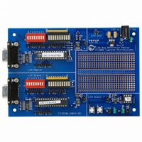
CY3220LINBUS-RD
Manufacturer Part Number
CY3220LINBUS-RD
Description
KIT REF DESIGN LIN BUS
Manufacturer
Cypress Semiconductor Corp
Series
PSoC®r
Datasheet
1.CY3220LINBUS-RD.pdf
(64 pages)
Specifications of CY3220LINBUS-RD
Main Purpose
Interface, LIN
Embedded
Yes, MCU, 8-Bit
Utilized Ic / Part
CY8C27143, CY8C27443
Processor To Be Evaluated
CY8C27143-24PXI and CY8C27443-24PXI
Interface Type
RS-232
Lead Free Status / RoHS Status
Contains lead / RoHS non-compliant
Lead Free Status / RoHS Status
Lead free / RoHS Compliant, Contains lead / RoHS non-compliant
Other names
428-1926


Contents
2
4.1 Slave Software Architecture .............................................................................................................. 31
3.4
3.5
3.6
3.7
3.8
4.2
4.3
4.4
4.5
4.6
Source Code Files ................................................................................................................... 18
Header Files ............................................................................................................................ 18
Creating a Project Using the Design IP ................................................................................... 18
3.6.1
3.6.2
3.6.3
3.6.4
3.6.5
3.6.6
3.6.7
3.6.8
3.6.9
3.6.10
3.6.11
3.6.12
3.6.13
Master Design APIs ................................................................................................................. 25
3.7.1
3.7.2
3.7.3
Time Study............................................................................................................................... 28
3.8.1
3.8.2
3.8.3
4.1.1
4.1.2
4.1.3
Device Configuration ............................................................................................................... 32
4.2.1
4.2.2
Firmware.................................................................................................................................. 32
4.3.1
4.3.2
4.3.3
4.3.4
4.3.5
4.3.6
4.3.7
LIN Source Code Files............................................................................................................. 34
Header Files ............................................................................................................................ 34
Using the Design IP ................................................................................................................. 35
4.6.1
4.6.2
4.6.3
4.6.4
4.6.5
Importing the Design ............................................................................................. 18
Configuring Global Resources............................................................................... 19
Configuring GPIO .................................................................................................. 19
Routing the Signals ............................................................................................... 19
Setting the Baud Rate ........................................................................................... 20
Adding the Schedule Timer ................................................................................... 20
Setting the Source Clock and Period .................................................................... 20
Configuring the Signal Table.................................................................................. 20
RAM Allocation ...................................................................................................... 20
Frame Definition .................................................................................................... 20
Schedule Table ...................................................................................................... 22
3.6.11.1
3.6.11.2
3.6.11.3
Adding the Main Application .................................................................................. 23
Special Features .................................................................................................... 23
3.6.13.1
3.6.13.2
3.6.13.3
Basic Functions ..................................................................................................... 25
Miscellaneous Core API Functions........................................................................ 26
LIN Node Configuration API Functions.................................................................. 27
ISR Timing ............................................................................................................. 28
Calculation of CPU Overhead Over a Frame ........................................................ 29
Maximum Interrupt Latency ................................................................................... 29
Overview................................................................................................................ 31
Foreground Processing ......................................................................................... 31
Timing and Interrupts ............................................................................................. 31
Synchro Reception Configuration .......................................................................... 32
Data Reception Configuration................................................................................ 32
Overview................................................................................................................ 32
GPIO Interrupt ....................................................................................................... 32
Synchro Timer Interrupt ......................................................................................... 33
Synchro Timeout Interrupt ..................................................................................... 33
RX Interrupt ...........................................................................................................33
TX Interrupt............................................................................................................ 34
Importing the Design ............................................................................................. 35
Configuring Global Resources............................................................................... 35
Configuring GPIO .................................................................................................. 35
Routing the Signals ............................................................................................... 36
Configuring the Signal Table.................................................................................. 36
Bit Timer Interrupt ................................................................................................. 34
Structure of Schedule Table ................................................................ 22
An Example Schedule Table ............................................................... 22
Diagnostic Schedules .......................................................................... 23
Low Power Management..................................................................... 23
Node Configuration.............................................................................. 24
Implementation of Sporadic Frames....................................................24
LIN Bus 2.0 Reference Design
Related parts for CY3220LINBUS-RD
Image
Part Number
Description
Manufacturer
Datasheet
Request
R

Part Number:
Description:
KIT DEMO PSOC CAPSENSE
Manufacturer:
Cypress Semiconductor Corp
Datasheet:

Part Number:
Description:
KIT DEMO PSOC CAPSENSE SLIDE
Manufacturer:
Cypress Semiconductor Corp

Part Number:
Description:
Manufacturer:
Cypress Semiconductor Corp
Datasheet:
Part Number:
Description:
Manufacturer:
Cypress Semiconductor Corp
Datasheet:
Part Number:
Description:
Manufacturer:
Cypress Semiconductor Corp
Datasheet:
Part Number:
Description:
Manufacturer:
Cypress Semiconductor Corp
Datasheet:
Part Number:
Description:
Manufacturer:
Cypress Semiconductor Corp
Datasheet: