CY3220LINBUS-RD Cypress Semiconductor Corp, CY3220LINBUS-RD Datasheet - Page 8
CY3220LINBUS-RD
Manufacturer Part Number
CY3220LINBUS-RD
Description
KIT REF DESIGN LIN BUS
Manufacturer
Cypress Semiconductor Corp
Series
PSoC®r
Datasheet
1.CY3220LINBUS-RD.pdf
(64 pages)
Specifications of CY3220LINBUS-RD
Main Purpose
Interface, LIN
Embedded
Yes, MCU, 8-Bit
Utilized Ic / Part
CY8C27143, CY8C27443
Processor To Be Evaluated
CY8C27143-24PXI and CY8C27443-24PXI
Interface Type
RS-232
Lead Free Status / RoHS Status
Contains lead / RoHS non-compliant
Lead Free Status / RoHS Status
Lead free / RoHS Compliant, Contains lead / RoHS non-compliant
Other names
428-1926


1. LIN Bus 2.0 Kit
LIN Bus 2.0 Reference Design
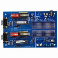
Power
Jack
Power
Supply
Master
Master
Serial Port
Node
Prototype
Area
Slave
1
Slave
2
Figure 1-1. LIN Bus Demonstration Board
The master node and slave 1 are both implemented in a 28-
pin part, CY8C27443-24PXI. Slave 2 is implemented in an
8-pin part, CY8C27143-24PXI.
The CD-ROM that is included with this kit has all project files
for the designed-in devices as well as project files for auto-
motive grade devices.
1.4
LIN Bus Demonstration
The LIN bus demonstration board is divided into four
regions: master node, slave 1, slave 2, and the prototype
area.
The master node has a bank of 8 dip-switches, SW2, and a
bank of 10 LEDs, U8. Slave 1 also has a set of 8 dip-
switches, SW1, and a bank of 10 LEDs, U7. Slave 2 has 2
push-button switches, S1 and S2, and 2 individual green
LEDs, D2 and D4. Figure 1-1 shows the positions of these
components.
6
Cypress Semiconductor – Rev. **
October 25, 2006
Related parts for CY3220LINBUS-RD
Image
Part Number
Description
Manufacturer
Datasheet
Request
R

Part Number:
Description:
KIT DEMO PSOC CAPSENSE
Manufacturer:
Cypress Semiconductor Corp
Datasheet:

Part Number:
Description:
KIT DEMO PSOC CAPSENSE SLIDE
Manufacturer:
Cypress Semiconductor Corp

Part Number:
Description:
Manufacturer:
Cypress Semiconductor Corp
Datasheet:
Part Number:
Description:
Manufacturer:
Cypress Semiconductor Corp
Datasheet:
Part Number:
Description:
Manufacturer:
Cypress Semiconductor Corp
Datasheet:
Part Number:
Description:
Manufacturer:
Cypress Semiconductor Corp
Datasheet:
Part Number:
Description:
Manufacturer:
Cypress Semiconductor Corp
Datasheet: