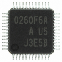
M30260F6AGP#U5A Renesas Electronics America, M30260F6AGP#U5A Datasheet - Page 127

M30260F6AGP#U5A
Manufacturer Part Number
M30260F6AGP#U5A
Description
IC M16C MCU FLASH 48K 48LQFP
Manufacturer
Renesas Electronics America
Series
M16C™ M16C/Tiny/26r
Datasheet
1.M30260F3AGPU5A.pdf
(354 pages)
Specifications of M30260F6AGP#U5A
Core Processor
M16C/60
Core Size
16-Bit
Speed
20MHz
Connectivity
I²C, IEBus, SIO, UART/USART
Peripherals
DMA, PWM, Voltage Detect, WDT
Number Of I /o
39
Program Memory Size
48KB (48K x 8)
Program Memory Type
FLASH
Ram Size
2K x 8
Voltage - Supply (vcc/vdd)
2.7 V ~ 5.5 V
Data Converters
A/D 12x10b
Oscillator Type
Internal
Operating Temperature
-20°C ~ 85°C
Package / Case
48-LQFP
Cpu Family
R8C
Device Core Size
16b
Frequency (max)
20MHz
Interface Type
UART
Total Internal Ram Size
2KB
# I/os (max)
39
Number Of Timers - General Purpose
8
Operating Supply Voltage (typ)
3.3/5V
Operating Supply Voltage (max)
5.5V
Operating Supply Voltage (min)
3V
On-chip Adc
12-chx10-bit
Instruction Set Architecture
CISC
Operating Temp Range
-20C to 85C
Operating Temperature Classification
Commercial
Mounting
Surface Mount
Pin Count
48
Package Type
LQFP
Package
48LQFP
Family Name
R8C
Maximum Speed
20 MHz
Operating Supply Voltage
3.3|5 V
Data Bus Width
16 Bit
Number Of Programmable I/os
39
Number Of Timers
8
For Use With
R0K33026AS000BE - KIT DEV EVALUATION M16C/26A
Lead Free Status / RoHS Status
Lead free / RoHS Compliant
Eeprom Size
-
Lead Free Status / Rohs Status
Compliant
Available stocks
Company
Part Number
Manufacturer
Quantity
Price
Part Number:
M30260F6AGP#U5AM30260F6AGP#D3
Manufacturer:
Renesas Electronics America
Quantity:
10 000
Part Number:
M30260F6AGP#U5AM30260F6AGP#U3
Manufacturer:
Renesas Electronics America
Quantity:
10 000
Part Number:
M30260F6AGP#U5AM30260F6AGP#U3A
Manufacturer:
Renesas Electronics America
Quantity:
10 000
- Current page: 127 of 354
- Download datasheet (4Mb)
R
R
M
12.2 Timer B
e
E
. v
J
1
Figure 12.2.1. Timer B Block Diagram
0
6
Figure 12.2.1 shows a block diagram of the timer B. Figures 12.2.2 and 12.2.3 show registers related to the
timer B.
Timer B supports the following four modes. Use the TMOD1 and TMOD0 bits in the TBiMR register (i = 0 to
2) to select the desired mode.
2
9
C
0 .
B
Note
The TB2
[Precautions when using Timer B2]
• Event Counter Mode
• Pulse Period/Pulse Width Measurement Mode
• Timer mode: The timer counts an internal count source.
• Event counter mode: The timer counts pulses from an external device or overflows or underflows of
• Pulse period/pulse width measuring mode: The timer measures an external signal's pulse period or
• A/D trigger mode: The timer starts counting by one trigger until the count value becomes 0000
0
2 /
0
This mode is used together with simultaneous sample sweep mode or delayed trigger mode 0 of A/D
converter to start A/D conversion.
other timers.
pulse width.
2
6
0
F
NOTE:
A
TBi
(i = 0 to 2)
2
e
0 -
b
G
1. Overflow or underflow.
IN
f
1 .
1
2
o r
0
or f
IN
, 5
f
Clock source selection
C32
0
f
u
32
f
2
pin for Timer B2 is not available in 42-pin package.
p
2
8
0
(
TBj overflow
0
Can be selected in
onlyevent counter mode
(j = i – 1, except j = 2 if i = 0)
M
7
1
Polarity switching,
edge pulse
6
page 108
C
2 /
6
(1)
, A
• Timer mode
• Pulse period/, pulse width measuring mode
• A/D trigger mode
• Event counter
The external input signals cannot be counted. Set the TCK1 bit in the
TB2MR register to “1” when using the Event Count Mode.
This mode connot be used.
M
f o
1
6
3
C
2
9
2 /
6
, B
M
1
6
C
2 /
Clock selection
6
) T
TABSR register
Counter reset circuit
Timer B0
Timer B1
Timer B2
TBi
Data bus high-order bits
Data bus low-order bits
Low-order 8 bits
Reload register
0391
0393
0395
Counter
Address
16
16
16
-
-
-
0390
0392
0394
16
16
16
Timer B2
Timer B0
Timer B1
High-order 8 bits
TBj
16
12. Timer
.
Related parts for M30260F6AGP#U5A
Image
Part Number
Description
Manufacturer
Datasheet
Request
R

Part Number:
Description:
KIT STARTER FOR M16C/29
Manufacturer:
Renesas Electronics America
Datasheet:

Part Number:
Description:
KIT STARTER FOR R8C/2D
Manufacturer:
Renesas Electronics America
Datasheet:

Part Number:
Description:
R0K33062P STARTER KIT
Manufacturer:
Renesas Electronics America
Datasheet:

Part Number:
Description:
KIT STARTER FOR R8C/23 E8A
Manufacturer:
Renesas Electronics America
Datasheet:

Part Number:
Description:
KIT STARTER FOR R8C/25
Manufacturer:
Renesas Electronics America
Datasheet:

Part Number:
Description:
KIT STARTER H8S2456 SHARPE DSPLY
Manufacturer:
Renesas Electronics America
Datasheet:

Part Number:
Description:
KIT STARTER FOR R8C38C
Manufacturer:
Renesas Electronics America
Datasheet:

Part Number:
Description:
KIT STARTER FOR R8C35C
Manufacturer:
Renesas Electronics America
Datasheet:

Part Number:
Description:
KIT STARTER FOR R8CL3AC+LCD APPS
Manufacturer:
Renesas Electronics America
Datasheet:

Part Number:
Description:
KIT STARTER FOR RX610
Manufacturer:
Renesas Electronics America
Datasheet:

Part Number:
Description:
KIT STARTER FOR R32C/118
Manufacturer:
Renesas Electronics America
Datasheet:

Part Number:
Description:
KIT DEV RSK-R8C/26-29
Manufacturer:
Renesas Electronics America
Datasheet:

Part Number:
Description:
KIT STARTER FOR SH7124
Manufacturer:
Renesas Electronics America
Datasheet:

Part Number:
Description:
KIT STARTER FOR H8SX/1622
Manufacturer:
Renesas Electronics America
Datasheet:

Part Number:
Description:
KIT DEV FOR SH7203
Manufacturer:
Renesas Electronics America
Datasheet:


