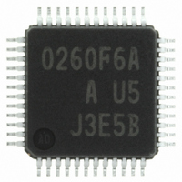
M30260F6AGP#U5A Renesas Electronics America, M30260F6AGP#U5A Datasheet - Page 36

M30260F6AGP#U5A
Manufacturer Part Number
M30260F6AGP#U5A
Description
IC M16C MCU FLASH 48K 48LQFP
Manufacturer
Renesas Electronics America
Series
M16C™ M16C/Tiny/26r
Datasheet
1.M30260F3AGPU5A.pdf
(354 pages)
Specifications of M30260F6AGP#U5A
Core Processor
M16C/60
Core Size
16-Bit
Speed
20MHz
Connectivity
I²C, IEBus, SIO, UART/USART
Peripherals
DMA, PWM, Voltage Detect, WDT
Number Of I /o
39
Program Memory Size
48KB (48K x 8)
Program Memory Type
FLASH
Ram Size
2K x 8
Voltage - Supply (vcc/vdd)
2.7 V ~ 5.5 V
Data Converters
A/D 12x10b
Oscillator Type
Internal
Operating Temperature
-20°C ~ 85°C
Package / Case
48-LQFP
Cpu Family
R8C
Device Core Size
16b
Frequency (max)
20MHz
Interface Type
UART
Total Internal Ram Size
2KB
# I/os (max)
39
Number Of Timers - General Purpose
8
Operating Supply Voltage (typ)
3.3/5V
Operating Supply Voltage (max)
5.5V
Operating Supply Voltage (min)
3V
On-chip Adc
12-chx10-bit
Instruction Set Architecture
CISC
Operating Temp Range
-20C to 85C
Operating Temperature Classification
Commercial
Mounting
Surface Mount
Pin Count
48
Package Type
LQFP
Package
48LQFP
Family Name
R8C
Maximum Speed
20 MHz
Operating Supply Voltage
3.3|5 V
Data Bus Width
16 Bit
Number Of Programmable I/os
39
Number Of Timers
8
For Use With
R0K33026AS000BE - KIT DEV EVALUATION M16C/26A
Lead Free Status / RoHS Status
Lead free / RoHS Compliant
Eeprom Size
-
Lead Free Status / Rohs Status
Compliant
Available stocks
Company
Part Number
Manufacturer
Quantity
Price
Part Number:
M30260F6AGP#U5AM30260F6AGP#D3
Manufacturer:
Renesas Electronics America
Quantity:
10 000
Part Number:
M30260F6AGP#U5AM30260F6AGP#U3
Manufacturer:
Renesas Electronics America
Quantity:
10 000
Part Number:
M30260F6AGP#U5AM30260F6AGP#U3A
Manufacturer:
Renesas Electronics America
Quantity:
10 000
- Current page: 36 of 354
- Download datasheet (4Mb)
M
R
R
2. Central Processing Unit (CPU)
e
E
1
. v
Figure 2.1. CPU Register
2.1 Data Registers (R0, R1, R2 and R3)
2.2 Address Registers (A0 and A1)
J
6
0
Figure 2.1 shows the CPU registers. The register bank is comprised of seven registers (R0, R1, R2, R3,
A0, A1 and FB) out of 13 registers. There are two sets of register bank.
The R0 register consists of 16 bits, and is used mainly for transfers and arithmetic/logic operations. R1 to
R3 are the same as R0.
The R0 register can be separated between high (R0H) and low (R0L) for use as two 8-bit data registers.
R1H and R1L are the same as R0H and R0L. Conversely, R2 and R0 can be combined for use as a 32-bit
data register (R2R0). R3R1 is the same as R2R0.
The register A0 consists of 16 bits, and is used for address register indirect addressing and address regis-
ter relative addressing. They also are used for transfers and arithmetic/logic operations. A1 is the same as
A0.
In some instructions, registers A1 and A0 can be combined for use as a 32-bit address register (A1A0).
C
2
9
0 .
2 /
B
0
0
6
2
A
0
F
2
e
G
0 -
b
o r
1 .
2
0
u
, 5
0
p
2
(
0
b31
M
0
1
7
6
C
page 17
2 /
6
NOTE:
, A
1. These registers comprise a register bank. There are two register banks.
R2
R3
M
b15
1
f o
6
C
3
2 /
2
b19
b19
The upper 4 bits of INTB are INTBH and
the lower 16 bits of INTB are INTBL.
9
INTBH
6
, B
M
b15
b15
b15
b15
R0H(R0's high bits)
R1H(R1's high bits)R1L(R1's low bits)
1
6
C
2 /
b8
6
b7
b
) T
PC
INTBL
USP
ISP
FLG
b8 b7
R2
R3
A0
A1
SB
FB
R0L(R0's low bits)
b0
b0
b0
b0
b0
b0
Flag register
Data registers (1)
Address registers (1)
Frame base registers (1)
Interrupt table register
Program counter
User stack pointer
Interrupt stack pointer
Static base register
Carry flag
Debug flag
Zero flag
Sign flag
Register bank select flag
Overflow flag
Interrupt enable flag
Stack pointer select flag
Reserved area
Processor interrupt priority level
Reserved area
2. CPU
Related parts for M30260F6AGP#U5A
Image
Part Number
Description
Manufacturer
Datasheet
Request
R

Part Number:
Description:
KIT STARTER FOR M16C/29
Manufacturer:
Renesas Electronics America
Datasheet:

Part Number:
Description:
KIT STARTER FOR R8C/2D
Manufacturer:
Renesas Electronics America
Datasheet:

Part Number:
Description:
R0K33062P STARTER KIT
Manufacturer:
Renesas Electronics America
Datasheet:

Part Number:
Description:
KIT STARTER FOR R8C/23 E8A
Manufacturer:
Renesas Electronics America
Datasheet:

Part Number:
Description:
KIT STARTER FOR R8C/25
Manufacturer:
Renesas Electronics America
Datasheet:

Part Number:
Description:
KIT STARTER H8S2456 SHARPE DSPLY
Manufacturer:
Renesas Electronics America
Datasheet:

Part Number:
Description:
KIT STARTER FOR R8C38C
Manufacturer:
Renesas Electronics America
Datasheet:

Part Number:
Description:
KIT STARTER FOR R8C35C
Manufacturer:
Renesas Electronics America
Datasheet:

Part Number:
Description:
KIT STARTER FOR R8CL3AC+LCD APPS
Manufacturer:
Renesas Electronics America
Datasheet:

Part Number:
Description:
KIT STARTER FOR RX610
Manufacturer:
Renesas Electronics America
Datasheet:

Part Number:
Description:
KIT STARTER FOR R32C/118
Manufacturer:
Renesas Electronics America
Datasheet:

Part Number:
Description:
KIT DEV RSK-R8C/26-29
Manufacturer:
Renesas Electronics America
Datasheet:

Part Number:
Description:
KIT STARTER FOR SH7124
Manufacturer:
Renesas Electronics America
Datasheet:

Part Number:
Description:
KIT STARTER FOR H8SX/1622
Manufacturer:
Renesas Electronics America
Datasheet:

Part Number:
Description:
KIT DEV FOR SH7203
Manufacturer:
Renesas Electronics America
Datasheet:


