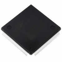
ST10F269Z2Q6 STMicroelectronics, ST10F269Z2Q6 Datasheet - Page 10

ST10F269Z2Q6
Manufacturer Part Number
ST10F269Z2Q6
Description
MCU 16BIT 256K FLASH 144PQFP
Manufacturer
STMicroelectronics
Series
ST10r
Specifications of ST10F269Z2Q6
Core Processor
ST10
Core Size
16-Bit
Speed
40MHz
Connectivity
CAN, EBI/EMI, SSC, UART/USART
Peripherals
POR, PWM, WDT
Number Of I /o
111
Program Memory Size
256KB (256K x 8)
Program Memory Type
FLASH
Ram Size
12K x 8
Voltage - Supply (vcc/vdd)
4.5 V ~ 5.5 V
Data Converters
A/D 16x10b
Oscillator Type
Internal
Operating Temperature
-40°C ~ 85°C
Package / Case
144-QFP
Controller Family/series
ST10
No. Of I/o's
111
Ram Memory Size
12KB
Cpu Speed
40MHz
No. Of Timers
5
Embedded Interface Type
CAN, SSC, USART
Rohs Compliant
Yes
Processor Series
ST10F26x
Core
ST10
Data Bus Width
16 bit
Data Ram Size
12 KB
Interface Type
CAN, SSC, USART
Maximum Clock Frequency
40 MHz
Number Of Programmable I/os
111
Number Of Timers
2 x 16 bit
Operating Supply Voltage
0.3 V to 4 V
Maximum Operating Temperature
+ 85 C
Mounting Style
SMD/SMT
Minimum Operating Temperature
- 40 C
On-chip Adc
16 bit x 10 bit
Lead Free Status / RoHS Status
Lead free / RoHS Compliant
Eeprom Size
-
Lead Free Status / Rohs Status
Details
Other names
497-4833
Available stocks
Company
Part Number
Manufacturer
Quantity
Price
Company:
Part Number:
ST10F269Z2Q6
Manufacturer:
ST
Quantity:
201
Company:
Part Number:
ST10F269Z2Q6
Manufacturer:
ST
Quantity:
745
Company:
Part Number:
ST10F269Z2Q6
Manufacturer:
STMicroelectronics
Quantity:
10 000
Part Number:
ST10F269Z2Q6
Manufacturer:
ST
Quantity:
20 000
2 - PIN DATA
10/184
P4.0 –P4.7
WR/WRL
READY/
Symbol
READY
ALE
RD
EA
85-92
Pin
85
86
87
88
89
90
91
92
95
96
97
98
99
Type
I/O
O
O
O
O
O
O
O
O
O
O
O
O
O
I
I
I
I
Port 4 is an 8-bit bidirectional I/O port. It is bit-wise programmable for input or output
via direction bit. Programming an I/O pin as input forces the corresponding output
driver to high impedance state. The input threshold is selectable (TTL or special).
Port 4.6 & 4.7 outputs can be configured as push-pull or open drain drivers.
In case of an external bus configuration, Port 4 can be used to output the segment
address lines:
P4.0
P4.1
P4.2
P4.3
P4.4
P4.5
P4.6
P4.7
External Memory Read Strobe. RD is activated for every external instruction or data
read access.
External Memory Write Strobe. In WR-mode this pin is activated for every external
data write access. In WRL mode this pin is activated for low Byte data write
accesses on a 16-bit bus, and for every data write access on an 8-bit bus. See
WRCFG in the SYSCON register for mode selection.
Ready Input. The active level is programmable. When the Ready function is
enabled, the selected inactive level at this pin, during an external memory access,
will force the insertion of waitstate cycles until the pin returns to the selected active
level.
Address Latch Enable Output. In case of use of external addressing or of multi-
plexed mode, this signal is the latch command of the address lines.
External Access Enable pin. A low level applied to this pin during and after Reset
forces the ST10F269 to start the program from the external memory space. A high
level forces the MCU to start in the internal memory space.
A16
A17
A18
A19
A20
CAN2_RxD
A21
CAN1_RxD
A22
CAN1_TxD
A23
CAN2_TxD
Segment Address Line
Segment Address Line
Segment Address Line
Segment Address Line
Segment Address Line
CAN2 Receive Data Input
Segment Address Line
CAN1 Receive Data Input
Segment Address Line
CAN1 Transmit Data Output
Most Significant Segment Address Line
CAN2 Transmit Data Output
Function
ST10F269


