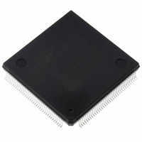
ST10F269Z2Q6 STMicroelectronics, ST10F269Z2Q6 Datasheet - Page 65

ST10F269Z2Q6
Manufacturer Part Number
ST10F269Z2Q6
Description
MCU 16BIT 256K FLASH 144PQFP
Manufacturer
STMicroelectronics
Series
ST10r
Specifications of ST10F269Z2Q6
Core Processor
ST10
Core Size
16-Bit
Speed
40MHz
Connectivity
CAN, EBI/EMI, SSC, UART/USART
Peripherals
POR, PWM, WDT
Number Of I /o
111
Program Memory Size
256KB (256K x 8)
Program Memory Type
FLASH
Ram Size
12K x 8
Voltage - Supply (vcc/vdd)
4.5 V ~ 5.5 V
Data Converters
A/D 16x10b
Oscillator Type
Internal
Operating Temperature
-40°C ~ 85°C
Package / Case
144-QFP
Controller Family/series
ST10
No. Of I/o's
111
Ram Memory Size
12KB
Cpu Speed
40MHz
No. Of Timers
5
Embedded Interface Type
CAN, SSC, USART
Rohs Compliant
Yes
Processor Series
ST10F26x
Core
ST10
Data Bus Width
16 bit
Data Ram Size
12 KB
Interface Type
CAN, SSC, USART
Maximum Clock Frequency
40 MHz
Number Of Programmable I/os
111
Number Of Timers
2 x 16 bit
Operating Supply Voltage
0.3 V to 4 V
Maximum Operating Temperature
+ 85 C
Mounting Style
SMD/SMT
Minimum Operating Temperature
- 40 C
On-chip Adc
16 bit x 10 bit
Lead Free Status / RoHS Status
Lead free / RoHS Compliant
Eeprom Size
-
Lead Free Status / Rohs Status
Details
Other names
497-4833
Available stocks
Company
Part Number
Manufacturer
Quantity
Price
Company:
Part Number:
ST10F269Z2Q6
Manufacturer:
ST
Quantity:
201
Company:
Part Number:
ST10F269Z2Q6
Manufacturer:
ST
Quantity:
745
Company:
Part Number:
ST10F269Z2Q6
Manufacturer:
STMicroelectronics
Quantity:
10 000
Part Number:
ST10F269Z2Q6
Manufacturer:
ST
Quantity:
20 000
ST10F269
When an external bus mode is enabled, the
direction of the port pin and the loading of data
into the port output latch are controlled by the bus
controller hardware.
The input of the port output Buffer is disconnected
from the internal bus and is switched to the line
labeled “Alternate Data Output” via a multiplexer.
The alternate data can be the 16-bit intra-segment
address or the 8/16-bit data information. The
incoming data on PORT0 is read on the line
Figure 22 : Block Diagram of a PORT0 Pin
Write P0H.y / P0L.y
Write DP0H.y / DP0L.y
Read DP0H.y / DP0L.y
Read P0H.y / P0L.y
Port Output
Direction
Latch
Latch
MUX
Alternate
Direction
Port Data
Output
1
0
Alternate
Function
Enable
Alternate
Data
Output
1
0
1
0
“Alternate Data Input”. While an external bus
mode is enabled, the user software should not
write
unpredictable results may occur.
When the external bus modes are disabled, the
contents of the direction register last written by the
user becomes active.
The Figure 22 shows the structure of a PORT0
pin.
MUX
MUX
to
the
Clock
Latch
Input
port
12 - PARALLEL PORTS
Output
Buffer
output
latch,
y = 7...0
otherwise
P0H.y
P0L.y
65/184


