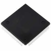
ST10F269Z2Q6 STMicroelectronics, ST10F269Z2Q6 Datasheet - Page 11

ST10F269Z2Q6
Manufacturer Part Number
ST10F269Z2Q6
Description
MCU 16BIT 256K FLASH 144PQFP
Manufacturer
STMicroelectronics
Series
ST10r
Specifications of ST10F269Z2Q6
Core Processor
ST10
Core Size
16-Bit
Speed
40MHz
Connectivity
CAN, EBI/EMI, SSC, UART/USART
Peripherals
POR, PWM, WDT
Number Of I /o
111
Program Memory Size
256KB (256K x 8)
Program Memory Type
FLASH
Ram Size
12K x 8
Voltage - Supply (vcc/vdd)
4.5 V ~ 5.5 V
Data Converters
A/D 16x10b
Oscillator Type
Internal
Operating Temperature
-40°C ~ 85°C
Package / Case
144-QFP
Controller Family/series
ST10
No. Of I/o's
111
Ram Memory Size
12KB
Cpu Speed
40MHz
No. Of Timers
5
Embedded Interface Type
CAN, SSC, USART
Rohs Compliant
Yes
Processor Series
ST10F26x
Core
ST10
Data Bus Width
16 bit
Data Ram Size
12 KB
Interface Type
CAN, SSC, USART
Maximum Clock Frequency
40 MHz
Number Of Programmable I/os
111
Number Of Timers
2 x 16 bit
Operating Supply Voltage
0.3 V to 4 V
Maximum Operating Temperature
+ 85 C
Mounting Style
SMD/SMT
Minimum Operating Temperature
- 40 C
On-chip Adc
16 bit x 10 bit
Lead Free Status / RoHS Status
Lead free / RoHS Compliant
Eeprom Size
-
Lead Free Status / Rohs Status
Details
Other names
497-4833
Available stocks
Company
Part Number
Manufacturer
Quantity
Price
Company:
Part Number:
ST10F269Z2Q6
Manufacturer:
ST
Quantity:
201
Company:
Part Number:
ST10F269Z2Q6
Manufacturer:
ST
Quantity:
745
Company:
Part Number:
ST10F269Z2Q6
Manufacturer:
STMicroelectronics
Quantity:
10 000
Part Number:
ST10F269Z2Q6
Manufacturer:
ST
Quantity:
20 000
ST10F269
P0L.0 - P0L.7,
P0H.1 - P0H.7
P1H.0 - P1H.7
P1L.0 - P1L.7
RSTOUT
Symbol
XTAL1
XTAL2
RSTIN
V
P0H.0
V
RPD
NMI
AGND
AREF
100-107,
111-117
118-125
128-135
108,
132
133
134
135
138
137
140
141
142
Pin
37
38
84
Type
I/O
I/O
O
O
-
-
-
I
I
I
I
I
I
I
Two 8-bit bidirectional I/O ports P0L and P0H, bit-wise programmable for input or
output via direction bit. Programming an I/O pin as input forces the corresponding
output driver to high impedance state.
In case of an external bus configuration, PORT0 serves as the address (A) and as
the address / data (AD) bus in multiplexed bus modes and as the data (D) bus in
demultiplexed bus modes.
Demultiplexed bus modes
Data Path Width:
P0L.0 – P0L.7:
P0H.0 – P0H.7
Multiplexed bus modes
Data Path Width:
P0L.0 – P0L.7:
P0H.0 – P0H.7
Two 8-bit bidirectional I/O ports P1L and P1H, bit-wise programmable for input or
output via direction bit. Programming an I/O pin as input forces the corresponding
output driver to high impedance state. PORT1 is used as the 16-bit address bus (A)
in demultiplexed bus modes and also after switching from a demultiplexed bus mode
to a multiplexed bus mode.
The following PORT1 pins have alternate functions:
P1H.4
P1H.5
P1H.6
P1H.7
XTAL1
XTAL2
To clock the device from an external source, drive XTAL1 while leaving XTAL2
unconnected. Minimum and maximum high / low and rise / fall times specified in the
AC Characteristics must be observed.
Reset Input with Schmitt-Trigger characteristics. A low level at this pin for a specified
duration while the oscillator is running resets the ST10F269. An internal pull-up
resistor permits power-on reset using only a capacitor connected to V
tional reset mode (enabled by setting bit BDRSTEN in SYSCON register), the
RSTIN line is pulled low for the duration of the internal reset sequence.
Internal Reset Indication Output. This pin is driven to a low level during hardware,
software or watchdog timer reset.
tialization) instruction is executed.
Non-Maskable Interrupt Input. A high to low transition at this pin causes the CPU to
vector to the NMI trap routine. If bit PWDCFG = ‘0’ in SYSCON register, when the
PWRDN (power down) instruction is executed, the NMI pin must be low in order to
force the ST10F269 to go into power down mode. If NMI is high and PWDCFG =’0’,
when PWRDN is executed, the part will continue to run in normal mode.
If not used, pin NMI should be pulled high externally.
A/D converter reference voltage.
A/D converter reference ground.
Timing pin for the return from interruptible powerdown mode and synchronous /
asynchronous reset selection.
CC24IO
CC25IO
CC26IO
CC27IO
Oscillator amplifier and/or external clock input.
Oscillator amplifier circuit output.
8-bit
D0 – D7
I/O
8-bit
A
A
D0 – AD7
8 – A15
CAPCOM2: CC24 Capture Input
CAPCOM2: CC25 Capture Input
CAPCOM2: CC26 Capture Input
CAPCOM2: CC27 Capture Input
16-bit
D0 - D7
D8 - D15
16-bit
A
A
RSTOUT
D0 - AD7
D8 - AD15
Function
remains low until the EINIT (end of ini-
2 - PIN DATA
SS
. In bidirec-
11/184


