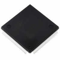
ST10F269Z2Q6 STMicroelectronics, ST10F269Z2Q6 Datasheet - Page 16

ST10F269Z2Q6
Manufacturer Part Number
ST10F269Z2Q6
Description
MCU 16BIT 256K FLASH 144PQFP
Manufacturer
STMicroelectronics
Series
ST10r
Specifications of ST10F269Z2Q6
Core Processor
ST10
Core Size
16-Bit
Speed
40MHz
Connectivity
CAN, EBI/EMI, SSC, UART/USART
Peripherals
POR, PWM, WDT
Number Of I /o
111
Program Memory Size
256KB (256K x 8)
Program Memory Type
FLASH
Ram Size
12K x 8
Voltage - Supply (vcc/vdd)
4.5 V ~ 5.5 V
Data Converters
A/D 16x10b
Oscillator Type
Internal
Operating Temperature
-40°C ~ 85°C
Package / Case
144-QFP
Controller Family/series
ST10
No. Of I/o's
111
Ram Memory Size
12KB
Cpu Speed
40MHz
No. Of Timers
5
Embedded Interface Type
CAN, SSC, USART
Rohs Compliant
Yes
Processor Series
ST10F26x
Core
ST10
Data Bus Width
16 bit
Data Ram Size
12 KB
Interface Type
CAN, SSC, USART
Maximum Clock Frequency
40 MHz
Number Of Programmable I/os
111
Number Of Timers
2 x 16 bit
Operating Supply Voltage
0.3 V to 4 V
Maximum Operating Temperature
+ 85 C
Mounting Style
SMD/SMT
Minimum Operating Temperature
- 40 C
On-chip Adc
16 bit x 10 bit
Lead Free Status / RoHS Status
Lead free / RoHS Compliant
Eeprom Size
-
Lead Free Status / Rohs Status
Details
Other names
497-4833
Available stocks
Company
Part Number
Manufacturer
Quantity
Price
Company:
Part Number:
ST10F269Z2Q6
Manufacturer:
ST
Quantity:
201
Company:
Part Number:
ST10F269Z2Q6
Manufacturer:
ST
Quantity:
745
Company:
Part Number:
ST10F269Z2Q6
Manufacturer:
STMicroelectronics
Quantity:
10 000
Part Number:
ST10F269Z2Q6
Manufacturer:
ST
Quantity:
20 000
4 - MEMORY ORGANIZATION
XPERCON (F024h / 12h)
Note: - When both CAN are disabled via XPER-
16/184
CAN1EN
CAN2EN
XRAM1EN
XRAM2EN
RTCEN
15
-
14
CON setting, then any access in the
address range 00’EE00h - 00’EFFFh will
be directed to external memory interface,
using the BUSCONx register correspond-
ing to address matching ADDRSELx regis-
ter. P4.4 and P4.7 can be used as General
Purpose I/O when CAN2 is disabled, and
P4.5 and P4.6 can be used as General
Purpose I/O when CAN1 is disabled.
- The default XPER selection after Reset is
identical
ST10C167: XCAN1 is enabled, XCAN2 is
disabled, XRAM1 (2K Byte compatible
XRAM) is enabled, XRAM2 (new 8K Byte
XRAM) is disabled.
- Register XPERCON cannot be changed
after the global enabling of XPeripherals,
i.e. after the setting of bit XPEN in the
SYSCON register.
- In EMUlation mode, all the XPERipherals
are enabled (XPERCON bit are all set).
-
13
-
CAN1 Enable Bit
‘0’: Accesses to the on-chip CAN1 XPeripheral and its functions are disabled. P4.5 and P4.6 pins can be
used as general purpose I/Os. Address range 00’EF00h-00’EFFFh is only directed to external memory if
CAN2EN is also ‘0’.
‘1’: The on-chip CAN1 XPeripheral is enabled and can be accessed.
CAN2 Enable Bit
‘0’: Accesses to the on-chip CAN2 XPeripheral and its functions are disabled. P4.4 and P4.7 pins can be
used as general purpose I/Os. Address range 00’EE00h-00’EEFFh is only directed to external memory if
CAN1EN is also ‘0’.
‘1’: The on-chip CAN2 XPeripheral is enabled and can be accessed.
XRAM1 Enable Bit
‘0’: Accesses to external memory within space 00’E000h to 00’E7FFh. The 2K Bytes of internal XRAM1
are disabled.
’1’: Accesses to the internal 2K Bytes of XRAM1.
XRAM2 Enable Bit
‘0’: Accesses to the external memory within space 00’C000h to 00’DFFFh. The 8K Bytes of internal
XRAM2 are disabled.
’1’: Accesses to the internal 8K Bytes of XRAM2.
RTC Enable Bit
’0’: Accesses to the on-chip Real Time Clock are disabled, external access is performed. Address range
00’EC00h-00’ECFFh is only directed to external memory if CAN1EN and CAN2EN are ’0’ also
’1’: The on-chip Real Time Clock is enabled and can be accessed.
12
-
to
11
-
XBUS
10
-
configuration
9
-
8
-
7
-
6
-
of
ESFR
5
-
RTCEN
RW
4
The access to external memory and/or
XBus is controlled by the bondout chip.
- When the Real Time Clock is disabled
(RTCEN = 0), the clock oscillator is
switch-off
power-down mode. Otherwise, when the
Real Time Clock is enabled, the bit
RTCOFF of the RTCCON register allows
to choose the power-down mode of the
clock oscillator (See Chapter : Real Time
Clock on page 105).
XRAM2EN
RW
3
if
XRAM1EN
RW
the
2
Reset Value: - - 05h
ST10
CAN2EN
RW
1
ST10F269
enters
CAN1EN
RW
0
in


