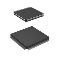
HD6417750RF240DV Renesas Electronics America, HD6417750RF240DV Datasheet - Page 377

HD6417750RF240DV
Manufacturer Part Number
HD6417750RF240DV
Description
MPU 3V 16K I-TEMP,PB-FREE 208-QF
Manufacturer
Renesas Electronics America
Series
SuperH® SH7750r
Datasheet
1.D6417750RBP240DV.pdf
(1164 pages)
Specifications of HD6417750RF240DV
Core Processor
SH-4
Core Size
32-Bit
Speed
240MHz
Connectivity
EBI/EMI, FIFO, SCI, SmartCard
Peripherals
DMA, POR, WDT
Number Of I /o
28
Program Memory Type
ROMless
Ram Size
48K x 8
Voltage - Supply (vcc/vdd)
1.4 V ~ 1.6 V
Oscillator Type
External
Operating Temperature
-40°C ~ 85°C
Package / Case
208-QFP
Lead Free Status / RoHS Status
Lead free / RoHS Compliant
Eeprom Size
-
Program Memory Size
-
Data Converters
-
Available stocks
Company
Part Number
Manufacturer
Quantity
Price
Company:
Part Number:
HD6417750RF240DV
Manufacturer:
HITACHI
Quantity:
7 287
- Current page: 377 of 1164
- Download datasheet (7Mb)
Section 10 Clock Oscillation Circuits
The function of each of the CPG blocks is described below.
PLL Circuit 1: PLL circuit 1 has a function for multiplying the clock frequency from the EXTAL
pin or crystal oscillation circuit by 6 with the SH7750 and SH7750S, and by 6 or 12 with the
SH7750R. Starting and stopping is controlled by a frequency control register setting. Control is
performed so that the internal clock rising edge phase matches the input clock rising edge phase.
PLL Circuit 2: PLL circuit 2 coordinates the phases of the bus clock and the CKIO pin output
clock. Starting and stopping is controlled by a frequency control register setting.
Crystal Oscillation Circuit: This is the oscillator circuit used when a crystal resonator is
connected to the XTAL and EXTAL pins. Use of the crystal oscillation circuit can be selected
with the MD8 pin.
Frequency Divider 1 (SH7750 and SH7750S only): Frequency divider 1 has a function for
adjusting the clock waveform duty to 50% by halving the input clock frequency when clock input
from the EXTAL pin is supplied internally without using PLL circuit 1.
Frequency Divider 2: Frequency divider 2 generates the CPU clock (Ick), bus clock (Bck), and
peripheral module clock (Pck). The division ratio is set in the frequency control register.
Clock Frequency Control Circuit: The clock frequency control circuit controls the clock
frequency by means of the MD pins and frequency control register.
Standby Control Circuit: The standby control circuit controls the state of the on-chip oscillation
circuits and other modules when the clock is switched and in sleep and standby modes.
Frequency Control Register (FRQCR): The frequency control register contains control bits for
clock output from the CKIO pin, PLL circuit 1 and 2 on/off control, and the CPU clock, bus clock,
and peripheral module clock frequency division ratios.
Standby Control Register (STBCR): The standby control register contains power save mode
control bits. For further information on the standby control register, see section 9, Power-Down
Modes.
Standby Control Register 2 (STBCR2): Standby control register 2 contains a power save mode
control bit. For further information on standby control register 2, see section 9, Power-Down
Modes.
Rev.7.00 Oct. 10, 2008 Page 291 of 1074
REJ09B0366-0700
Related parts for HD6417750RF240DV
Image
Part Number
Description
Manufacturer
Datasheet
Request
R

Part Number:
Description:
KIT STARTER FOR M16C/29
Manufacturer:
Renesas Electronics America
Datasheet:

Part Number:
Description:
KIT STARTER FOR R8C/2D
Manufacturer:
Renesas Electronics America
Datasheet:

Part Number:
Description:
R0K33062P STARTER KIT
Manufacturer:
Renesas Electronics America
Datasheet:

Part Number:
Description:
KIT STARTER FOR R8C/23 E8A
Manufacturer:
Renesas Electronics America
Datasheet:

Part Number:
Description:
KIT STARTER FOR R8C/25
Manufacturer:
Renesas Electronics America
Datasheet:

Part Number:
Description:
KIT STARTER H8S2456 SHARPE DSPLY
Manufacturer:
Renesas Electronics America
Datasheet:

Part Number:
Description:
KIT STARTER FOR R8C38C
Manufacturer:
Renesas Electronics America
Datasheet:

Part Number:
Description:
KIT STARTER FOR R8C35C
Manufacturer:
Renesas Electronics America
Datasheet:

Part Number:
Description:
KIT STARTER FOR R8CL3AC+LCD APPS
Manufacturer:
Renesas Electronics America
Datasheet:

Part Number:
Description:
KIT STARTER FOR RX610
Manufacturer:
Renesas Electronics America
Datasheet:

Part Number:
Description:
KIT STARTER FOR R32C/118
Manufacturer:
Renesas Electronics America
Datasheet:

Part Number:
Description:
KIT DEV RSK-R8C/26-29
Manufacturer:
Renesas Electronics America
Datasheet:

Part Number:
Description:
KIT STARTER FOR SH7124
Manufacturer:
Renesas Electronics America
Datasheet:

Part Number:
Description:
KIT STARTER FOR H8SX/1622
Manufacturer:
Renesas Electronics America
Datasheet:

Part Number:
Description:
KIT DEV FOR SH7203
Manufacturer:
Renesas Electronics America
Datasheet:


