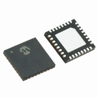
MRF89XA-I/MQ Microchip Technology, MRF89XA-I/MQ Datasheet - Page 102

MRF89XA-I/MQ
Manufacturer Part Number
MRF89XA-I/MQ
Description
TXRX ISM SUB-GHZ ULP 32QFN
Manufacturer
Microchip Technology
Specifications of MRF89XA-I/MQ
Package / Case
32-WFQFN Exposed Pad
Frequency
863MHz ~ 870MHz, 902MHz ~ 928MHz, 950MHz ~ 960MHz
Data Rate - Maximum
200kbps
Modulation Or Protocol
FSK, OOK
Applications
ISM
Power - Output
12.5dBm
Sensitivity
-113dBm
Voltage - Supply
2.1 V ~ 3.6 V
Current - Receiving
3mA
Current - Transmitting
25mA
Data Interface
PCB, Surface Mount
Antenna Connector
PCB, Surface Mount
Operating Temperature
-40°C ~ 85°C
Number Of Receivers
1
Number Of Transmitters
1
Wireless Frequency
863 MHz to 870 MHz, 902 MHz to 928 MHz, 950 MHz to 960 MHz
Interface Type
SPI
Noise Figure
- 112 dBc
Output Power
- 8.5 dBm, + 12.5 dBm
Operating Supply Voltage
2.1 V to 3.6 V
Maximum Operating Temperature
+ 85 C
Mounting Style
SMD/SMT
Maximum Data Rate
256 Kbps
Maximum Supply Current
25 mA
Minimum Operating Temperature
- 40 C
Modulation
FSK
Lead Free Status / RoHS Status
Lead free / RoHS Compliant
Memory Size
-
Lead Free Status / Rohs Status
Lead free / RoHS Compliant
Available stocks
Company
Part Number
Manufacturer
Quantity
Price
Company:
Part Number:
MRF89XA-I/MQ
Manufacturer:
MICROCHIP
Quantity:
12 000
4.4.4
To adequately reject spurious components arising from
the comparison frequency F
order loop filter is used. Figure 4-7 illustrates the loop
filter circuit.
FIGURE 4-7:
The recommendations made in Section 3.2.4.1 “PLL
Requirements” and the loop filter proposed in the
application schematic’s BOM in Section 4.7 “Bill of
Materials” can be used. The loop filter settings are fre-
quency band independent and are hence relevant to all
implementations of the MRF89XA.
4.4.5
The integrated VCO requires only two external tank cir-
cuit inductors. As the input is differential, the two induc-
tors should have the same nominal value. The
performance of these components is important for both
the phase noise and the power consumption of the
PLL.
TABLE 4-2:
DS70622B-page 102
MRF89XA
f
CLOAD
R
C
Δf
Δf
Δf
xtal
Note:
M
O
xtal
xtal
xtal
CL2
(ΔT)
(Δt)
Name
PLL LOOP FILTER
VOLTAGE CONTROLLED
OSCILLATOR (VCO)
The initial frequency tolerance, temperature stability and ageing performance should be chosen in
accordance with the target operating temperature range and the receiver bandwidth selected.
RL1
CRYSTAL RESONATOR SPECIFICATION
Nominal frequency
Load capacitance for f
Motional resistance
Shunt capacitance
Calibration tolerance at 25+/-3°C
Stability over temperature range [-40°C; +85°C]
Aging (first year)
CL1
Loop Filter
COMP
, an external second
PLLP
PLLN
Description
xtal
Preliminary
It is recommended that a pair of high Q factor inductors
is selected. These should be mounted orthogonally to
other inductors (in particular the PA choke) to reduce
spurious coupling between the PA and VCO. These
measures may reduce radiated pulling effects and
undesirable transient behavior, thus minimizing spec-
tral occupancy. Ensuring a symmetrical layout of the
VCO inductors will improve PLL spectral purity.
4.5
During the Reset event (caused by power-on, a glitch
on the supply line or a software Reset), the V
should be kept clean. Noise or a periodic disturbing sig-
nal superimposed on the supply voltage may prevent
the device from getting out of the Reset state. To avoid
this, adequate filters should be made available on the
power supply lines to keep the distorting signal level
below 100-150 mV peak-to-peak, in the DC to 50 kHz
range for 200 ms, from V
regulators or switching power supplies may sometimes
introduce switching noise on the V
the power supply manufacturer’s recommendations on
how to decrease the ripple of regulator IC and/or how
to shift the switching frequency.
4.6
Table 4-2 lists the crystal resonator specification for the
crystal reference oscillator circuit of the MRF89XA.
This specification covers the full range of operation of
the MRF89XA and is used in the application schematic
(for more information, see Section 4.7 “Bill of Materi-
als”).
Minimum
V
Crystal Specification and
Selection Guidelines
DD
-15
-20
10
—
9
1
5
Line Filtering
Typical
12.800
15
—
—
—
—
—
© 2010 Microchip Technology Inc.
DD
ramp start. The usage of
Maximum
DD
16.5
100
+15
+20
15
7
5
line, hence follow
Ohms
Units
MHz
ppm
ppm
ppm
pF
pF
DD
line


