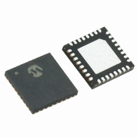
MRF89XA-I/MQ Microchip Technology, MRF89XA-I/MQ Datasheet - Page 30

MRF89XA-I/MQ
Manufacturer Part Number
MRF89XA-I/MQ
Description
TXRX ISM SUB-GHZ ULP 32QFN
Manufacturer
Microchip Technology
Specifications of MRF89XA-I/MQ
Package / Case
32-WFQFN Exposed Pad
Frequency
863MHz ~ 870MHz, 902MHz ~ 928MHz, 950MHz ~ 960MHz
Data Rate - Maximum
200kbps
Modulation Or Protocol
FSK, OOK
Applications
ISM
Power - Output
12.5dBm
Sensitivity
-113dBm
Voltage - Supply
2.1 V ~ 3.6 V
Current - Receiving
3mA
Current - Transmitting
25mA
Data Interface
PCB, Surface Mount
Antenna Connector
PCB, Surface Mount
Operating Temperature
-40°C ~ 85°C
Number Of Receivers
1
Number Of Transmitters
1
Wireless Frequency
863 MHz to 870 MHz, 902 MHz to 928 MHz, 950 MHz to 960 MHz
Interface Type
SPI
Noise Figure
- 112 dBc
Output Power
- 8.5 dBm, + 12.5 dBm
Operating Supply Voltage
2.1 V to 3.6 V
Maximum Operating Temperature
+ 85 C
Mounting Style
SMD/SMT
Maximum Data Rate
256 Kbps
Maximum Supply Current
25 mA
Minimum Operating Temperature
- 40 C
Modulation
FSK
Lead Free Status / RoHS Status
Lead free / RoHS Compliant
Memory Size
-
Lead Free Status / Rohs Status
Lead free / RoHS Compliant
Available stocks
Company
Part Number
Manufacturer
Quantity
Price
Company:
Part Number:
MRF89XA-I/MQ
Manufacturer:
MICROCHIP
Quantity:
12 000
TABLE 2-6:
DS70622B-page 30
MRF89XA
General Configuration Registers: Size – 13 Bytes, Start Address – 0x00
Interrupt Configuration Registers: Size – 3 Bytes, Start Address – 0x0D
Receiver Configuration Registers: Size – 6 Bytes, Start Address – 0x10
Register
Address
Register
Address
Register
Address
0x0A
0x0B
0x0C
0x0D
0x0E
0x0F
0x00
0x01
0x02
0x03
0x04
0x05
0x06
0x07
0x08
0x09
0x10
0x11
0x12
0x13
GCONREG
DMODREG
FDEVREG
BRSREG
FLTHREG
FIFOCREG
R1CREG
P1CREG
S1CREG
R2CREG
P2CREG
S2CREG
PACREG
FTXRXIREG
FTPRIREG
RSTHIREG
FILCREG
PFCREG
SYNCREG
RESVREG
Register
Register
Register
Name
Name
Name
CONFIGURATION/CONTROL/STATUS REGISTER DESCRIPTION
General Configuration Register
Data and Modulation Configuration
Register
Frequency Deviation Control Register
Bit Rate Set Register
Floor Threshold Control Register
FIFO Configuration Register
R1 Counter Set Register
P1 Counter Set Register
S1 Counter Set Register
R2 Counter Set Register
P2 Counter Set Register
S2 Counter Set Register
Power Amplifier Control Register
FIFO, Transmit and Receive Interrupt
Request Configuration Register
FIFO Transmit PLL and RSSI Interrupt
Configuration Register
RSSI Threshold Interrupt Request
Configuration Register
Filter Configuration Register
Polyphase Filter Configuration Register
Sync Control Register
Reserved Register
Register Description
Register Description
Register Description
Preliminary
Transceiver mode, frequency band
selection, VCO trimming, PLL frequency
dividers selection
Modulation type, Data mode, OOK
threshold type, IF gain
Frequency deviation in FSK Transmit mode
Operational bit rate
Floor threshold in OOK Receive mode
FIFO size and threshold
Value input for R1 counter
Value input for P1 counter
Value input for S1 counter
Value input for R2 counter
Value input for P2 counter
Value input for S2 counter
Ramp Control of PA regulator output
voltage in OOK
Interrupt request (IRQ0 and IRQ1) in
Receive mode, interrupt request (IRQ1) in
Transmit mode, interrupt request for FIFO
full, empty and overrun
FIFO fill method, FIFO fill, interrupt request
(IRQ0) for transmit start, interrupt request
for RSSI, PLL lock enable and status
RSSI threshold for interrupt
Passive filter bandwidth selection, sets the
receiver bandwidth
(Butterworth filter)
Selects the central frequency of the
polyphase filter
Enables polyphase filter (in OOK receive
mode, bit synchronizer control, Sync word
recognition, Sync word size, Sync word
error
Reserved for future use
Related Control Functions
Related Control Functions
Related Control Functions
© 2010 Microchip Technology Inc.


