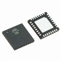
MRF89XA-I/MQ Microchip Technology, MRF89XA-I/MQ Datasheet - Page 14

MRF89XA-I/MQ
Manufacturer Part Number
MRF89XA-I/MQ
Description
TXRX ISM SUB-GHZ ULP 32QFN
Manufacturer
Microchip Technology
Specifications of MRF89XA-I/MQ
Package / Case
32-WFQFN Exposed Pad
Frequency
863MHz ~ 870MHz, 902MHz ~ 928MHz, 950MHz ~ 960MHz
Data Rate - Maximum
200kbps
Modulation Or Protocol
FSK, OOK
Applications
ISM
Power - Output
12.5dBm
Sensitivity
-113dBm
Voltage - Supply
2.1 V ~ 3.6 V
Current - Receiving
3mA
Current - Transmitting
25mA
Data Interface
PCB, Surface Mount
Antenna Connector
PCB, Surface Mount
Operating Temperature
-40°C ~ 85°C
Number Of Receivers
1
Number Of Transmitters
1
Wireless Frequency
863 MHz to 870 MHz, 902 MHz to 928 MHz, 950 MHz to 960 MHz
Interface Type
SPI
Noise Figure
- 112 dBc
Output Power
- 8.5 dBm, + 12.5 dBm
Operating Supply Voltage
2.1 V to 3.6 V
Maximum Operating Temperature
+ 85 C
Mounting Style
SMD/SMT
Maximum Data Rate
256 Kbps
Maximum Supply Current
25 mA
Minimum Operating Temperature
- 40 C
Modulation
FSK
Lead Free Status / RoHS Status
Lead free / RoHS Compliant
Memory Size
-
Lead Free Status / Rohs Status
Lead free / RoHS Compliant
Available stocks
Company
Part Number
Manufacturer
Quantity
Price
Company:
Part Number:
MRF89XA-I/MQ
Manufacturer:
MICROCHIP
Quantity:
12 000
2.1
To
characteristics over a wide supply range, the
MRF89XA is internally voltage regulated. This internal
regulated power supply block structure is illustrated in
Figure 2-2.
The power supply bypassing is essential for better
handling of signal surges and noise in the power line.
To ensure correct operation of the regulator circuit, the
decoupling capacitor connection (shown in Figure 2-2)
is recommended. These decoupling components are
recommended for any design. The power supply block
generates four regulated supplies for the analog,
digital, VCO and the PLL blocks to reduce the voltages
for their specific requirements. However, Power-on
Reset (POR), Configuration registers and the SPI use
the V
FIGURE 2-2:
TABLE 2-2:
DS70622B-page 14
MRF89XA
POR, SPI and Configuration Registers
Regulated Supply (V
Analog
Digital
VCO
PA
DD
provide
supply given to the MRF89XA.
Power Supply and Ground Block
Pins
Biasing:
- SPI
- Config. Registers
- POR
Blocks
stable
POWER SUPPLY PIN DETAILS
INTS
POWER SUPPLY BLOCK DIAGRAM
)
sensitivity
V
BAT
1 µF
Analog Regulator
Y5V
Biasing Analog
Blocks
1.0 V
and
AVRS
Pin 27
Biasing Through
linearity
Y5V
1 µF
V
V
V
Preliminary
0.22 µF
V
V
V
INTS
INTS
INTS
Digital Regulator
X7R
Internal Regulator
DD
DD
DD
Biasing Digital
Blocks
1.4 V
1.0 V
DVRS
Pin 28
External Supply
V
The large value decoupling capacitors should be
placed at the PCB power input. The smaller value
decoupling capacitors should be placed at every power
point of the device and at bias points for the RF port.
Poor bypassing can lead to conducted interference,
which can cause noise and spurious signals to couple
into the RF sections, thereby significantly reducing the
performance.
It is recommended that the V
capacitors to ensure sufficient bypass and decoupling.
However, based on the selected carrier frequency, the
bypass capacitor values vary. The trace length (V
to bypass capacitors) should be made as short as
possible.
DD
2.1 – 3.6V
– Pin 26
0.1 µF
Associated Pins
X7R
VCO Regulator
V
Biasing:
- VCO Circuit
- Ext. VCO Tank
INTS
VCORS
0.85 V
DVRS
AVRS
PARS
V
V
DD
DD
VCORS
Pin 3
© 2010 Microchip Technology Inc.
0.047 µF
Biasing:
- PA Driver
- Ext. PA Choke
X7R
PA Regulator
DD
1.80 V
Regulated Voltage
pin have two bypass
Pin 29
PARS
(in Volts)
2.1-3.6
0.85
1.4
1.0
1.0
1.8
DD
pin


