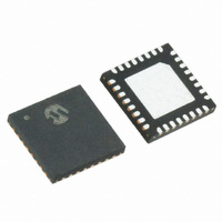
MRF89XA-I/MQ Microchip Technology, MRF89XA-I/MQ Datasheet - Page 77

MRF89XA-I/MQ
Manufacturer Part Number
MRF89XA-I/MQ
Description
TXRX ISM SUB-GHZ ULP 32QFN
Manufacturer
Microchip Technology
Specifications of MRF89XA-I/MQ
Package / Case
32-WFQFN Exposed Pad
Frequency
863MHz ~ 870MHz, 902MHz ~ 928MHz, 950MHz ~ 960MHz
Data Rate - Maximum
200kbps
Modulation Or Protocol
FSK, OOK
Applications
ISM
Power - Output
12.5dBm
Sensitivity
-113dBm
Voltage - Supply
2.1 V ~ 3.6 V
Current - Receiving
3mA
Current - Transmitting
25mA
Data Interface
PCB, Surface Mount
Antenna Connector
PCB, Surface Mount
Operating Temperature
-40°C ~ 85°C
Number Of Receivers
1
Number Of Transmitters
1
Wireless Frequency
863 MHz to 870 MHz, 902 MHz to 928 MHz, 950 MHz to 960 MHz
Interface Type
SPI
Noise Figure
- 112 dBc
Output Power
- 8.5 dBm, + 12.5 dBm
Operating Supply Voltage
2.1 V to 3.6 V
Maximum Operating Temperature
+ 85 C
Mounting Style
SMD/SMT
Maximum Data Rate
256 Kbps
Maximum Supply Current
25 mA
Minimum Operating Temperature
- 40 C
Modulation
FSK
Lead Free Status / RoHS Status
Lead free / RoHS Compliant
Memory Size
-
Lead Free Status / Rohs Status
Lead free / RoHS Compliant
Available stocks
Company
Part Number
Manufacturer
Quantity
Price
Company:
Part Number:
MRF89XA-I/MQ
Manufacturer:
MICROCHIP
Quantity:
12 000
3.8
3.8.1
The MRF89XA data processing blocks are as
illustrated in the Figure 3-16. Its role is to interface the
data to/from the modulator/demodulator and the host
microcontroller access points (SPI, Interrupts (IRQ0
and IRQ1), DATA pins). It also controls all the configu-
ration registers.
The circuit contains several control blocks which are
described in the following paragraphs.
The MRF89XA implements several data operation
modes, each with their own data path through the data
processing section. Depending on the data operation
mode selected, some control blocks are active while
others remain disabled.
FIGURE 3-16:
TABLE 3-4:
© 2010 Microchip Technology Inc.
Continuous
Buffered
Packet
Data Operation Mode
Data
Data Processing
DATA PROCESSING BLOCK
DIAGRAM
TX/RX
RX
TX
DATA OPERATION MODE SELECTION
Recognition
MRF89XA DATA PROCESSING BLOCK DIAGRAM
SYNC
Handler
Packet
DMODE1
0
0
1
MRF89XA
Preliminary
Control
(+SR)
FIFO
3.8.2
The MRF89XA has three different data operation
modes which can be selected by the user or
programmer:
• Continuous mode: Each bit transmitted or
• Buffered mode: Each byte transmitted or received
• Packet mode (recommended): User only pro-
received is accessed in real time at the DATA pin.
This mode may be used if adequate external sig-
nal processing is available.
is stored in a FIFO and accessed through the SPI
bus. The host microcontroller processing over-
head reduced significantly compared to Continu-
ous mode operation. The packet length is
unlimited.
vides/retrieves payload bytes to/from the FIFO.
The packet is automatically built with preamble,
Sync word, and optional CRC, DC free encoding
and the reverse operation is performed in recep-
tion. The host microcontroller processing over-
head is further reduced compared to Buffered
mode. The maximum payload length is limited to
the maximum FIFO limit of 64 bytes.
DMODE0
0
1
x
DATA OPERATION MODES
CONFIG
DATA
SPI
MRF89XA
FTXRXIREG
FTXRXIREG
FTXRXIREG
Register
DS70622B-page 77
SDO
CSDAT
SCK
SDI
DATA
IRQ1
IRQ0


