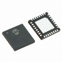
MRF89XA-I/MQ Microchip Technology, MRF89XA-I/MQ Datasheet - Page 74

MRF89XA-I/MQ
Manufacturer Part Number
MRF89XA-I/MQ
Description
TXRX ISM SUB-GHZ ULP 32QFN
Manufacturer
Microchip Technology
Specifications of MRF89XA-I/MQ
Package / Case
32-WFQFN Exposed Pad
Frequency
863MHz ~ 870MHz, 902MHz ~ 928MHz, 950MHz ~ 960MHz
Data Rate - Maximum
200kbps
Modulation Or Protocol
FSK, OOK
Applications
ISM
Power - Output
12.5dBm
Sensitivity
-113dBm
Voltage - Supply
2.1 V ~ 3.6 V
Current - Receiving
3mA
Current - Transmitting
25mA
Data Interface
PCB, Surface Mount
Antenna Connector
PCB, Surface Mount
Operating Temperature
-40°C ~ 85°C
Number Of Receivers
1
Number Of Transmitters
1
Wireless Frequency
863 MHz to 870 MHz, 902 MHz to 928 MHz, 950 MHz to 960 MHz
Interface Type
SPI
Noise Figure
- 112 dBc
Output Power
- 8.5 dBm, + 12.5 dBm
Operating Supply Voltage
2.1 V to 3.6 V
Maximum Operating Temperature
+ 85 C
Mounting Style
SMD/SMT
Maximum Data Rate
256 Kbps
Maximum Supply Current
25 mA
Minimum Operating Temperature
- 40 C
Modulation
FSK
Lead Free Status / RoHS Status
Lead free / RoHS Compliant
Memory Size
-
Lead Free Status / Rohs Status
Lead free / RoHS Compliant
Available stocks
Company
Part Number
Manufacturer
Quantity
Price
Company:
Part Number:
MRF89XA-I/MQ
Manufacturer:
MICROCHIP
Quantity:
12 000
3.4.13
After OOK or FSK demodulation, the baseband signal
is made available to the user on the DATA pin (pin 20),
when Continuous mode is selected. In Buffered and
Packet modes, the data is retrieved from the FIFO
through the SPI.
During Receive mode, the received data is filled into
the Shift register and then transferred onto the FIFO
stack. The FIFO is configured to generate an interrupt
after receiving a defined number of bits.
When the internal FIFO is enabled, the FIFO interrupt,
which is configured through the IRQ0 and IRQ1 pins
(pin 21 and 22), acts as a FIFOFULL interrupt,
indicating that the FIFO has been filled to its
preprogrammed limit. The receiver starts filling the
FIFO with data when it identifies the synchronous
pattern through the synchronous pattern recognition
circuit. It is recommended to set the threshold to at
least half the length of the register (8 bits) to ensure that
the external host microcontroller has time to set up.
The synchronous pattern recognition circuit prevents
the FIFO from being filled up with noise, and therefore
avoids overloading the external host microcontroller.
3.4.14
The registers associated with Receive mode are:
• GCONREG (Register 2-1)
• DMODREG (Register 2-2)
• FDEVREG (Register 2-3)
• BRSREG (Register 2-4)
• FLTHREG (Register 2-5)
• FIFOCREG (Register 2-6)
• FTXRXIREG (Register 2-14)
• FTPRIREG (Register 2-14)
• RSTHIREG (Register 2-16)
• FILCREG (Register 2-17)
• PFCREG (Register 2-18)
• SYNCREG (Register 2-19)
• RSTSREG (Register 2-21)
• OOKCREG (Register 2-22)
• SYNCV31REG (Register 2-23)
• SYNCV23REG (Register 2-24)
• SYNCV15REG (Register 2-25)
• SYNCV07REG (Register 2-26)
DS70622B-page 74
MRF89XA
DATA OUTPUT
RECEIVE MODE REGISTERS
Preliminary
3.5
3.5.1
For more information on standard SPI between the
MRF89XA and a Microcontroller, refer to Section 2.11
“Serial Peripheral Interface (SPI)”.
3.5.2
The registers associated with SPI communication are:
• GCONREG (Register 2-1)
• DMODREG (Register 2-2)
• FDEVREG (Register 2-3)
• BRSREG (Register 2-4)
3.6
The hardware description of the FIFO is described in
Section 2.12 “FIFO and Shift Register (SR)”. The
FIFO is handled by selecting the size of the FIFO, FIFO
interrupts, and clearing the FIFO.
3.6.1
The FIFO width is programmable to 16, 32, 48 or 64
bytes using the FSIZE<1:0> bits (FIFOCREG<7:6>).
3.6.2
The MRF89XA generates an interrupt request for the
host microcontroller by pulling the IRQ0 or IRQ1 pins
low or high based on the events and configuration set-
tings of these interrupts. All interrupt sources and flags
are configured through the Interrupt Configuration reg-
isters, based on the occurrence of the following events:
• Interrupt Requests (IRQ0 and IRQ1) during differ-
• Interrupt Requests (IRQ0 and IRQ1) during trans-
ent receive stand-by data modes (such as Contin-
uous, Buffer and Packet) for following event
occurrences: SYNC, RSSI, PLREADY, ARDS-
MATCH and /FIFOEMPTY.
For example, Write Byte. The WRITEBYTE inter-
rupt source goes high for one bit period each time
a new byte is transferred from the shift register to
the FIFO (that is, each time a new byte is
received).
mit modes (such as Continuous, Buffer and
Packet) for the following event occurrences: Data
Clock, FIFOFULL, Transmit Done, Transmit Start
with IRQ0 and IRQ1.
For example, TX Done. The TXDONE interrupt
source goes high when the FIFO is empty and the
Shift register’s last bit has been sent to the modu-
lator (that is, the last bit of the packet has been
sent). One bit period delay is required after the ris-
ing edge of TXDONE to ensure correct RF trans-
mission of the last bit. In practice this may not
require special care in the MCU software due to
IRQ processing time.
Control Block Description
FIFO Handling
SPI INTERFACE
SPI REGISTERS
SIZE SELECTION
INTERRUPT SOURCES AND FLAGS
© 2010 Microchip Technology Inc.


