MRF89XA-I/MQ Microchip Technology, MRF89XA-I/MQ Datasheet - Page 4
MRF89XA-I/MQ
Manufacturer Part Number
MRF89XA-I/MQ
Description
TXRX ISM SUB-GHZ ULP 32QFN
Manufacturer
Microchip Technology
Specifications of MRF89XA-I/MQ
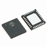
Package / Case
32-WFQFN Exposed Pad
Frequency
863MHz ~ 870MHz, 902MHz ~ 928MHz, 950MHz ~ 960MHz
Data Rate - Maximum
200kbps
Modulation Or Protocol
FSK, OOK
Applications
ISM
Power - Output
12.5dBm
Sensitivity
-113dBm
Voltage - Supply
2.1 V ~ 3.6 V
Current - Receiving
3mA
Current - Transmitting
25mA
Data Interface
PCB, Surface Mount
Antenna Connector
PCB, Surface Mount
Operating Temperature
-40°C ~ 85°C
Number Of Receivers
1
Number Of Transmitters
1
Wireless Frequency
863 MHz to 870 MHz, 902 MHz to 928 MHz, 950 MHz to 960 MHz
Interface Type
SPI
Noise Figure
- 112 dBc
Output Power
- 8.5 dBm, + 12.5 dBm
Operating Supply Voltage
2.1 V to 3.6 V
Maximum Operating Temperature
+ 85 C
Mounting Style
SMD/SMT
Maximum Data Rate
256 Kbps
Maximum Supply Current
25 mA
Minimum Operating Temperature
- 40 C
Modulation
FSK
Lead Free Status / RoHS Status
Lead free / RoHS Compliant
Memory Size
-
Lead Free Status / Rohs Status
Lead free / RoHS Compliant
Available stocks
Company
Part Number
Manufacturer
Quantity
Price
Company:

Part Number:
MRF89XA-I/MQ
Manufacturer:
MICROCHIP
Quantity:
12 000


MRF89XA
All critical RF and baseband functions are integrated in
the MRF89XA, minimizing the external component
count
communication parameters are made programmable
and most of them may be dynamically set. A
microcontroller, RF SAW filter, 12.8 MHz crystal, and a
few passive components are all that are needed to
create a complete, reliable radio function. The
MRF89XA uses several low-power mechanisms to
reduce overall current consumption and extend battery
life. Its small size and low power consumption makes
the MRF89XA ideal for a wide variety of short range
radio applications. The MRF89XA complies with
European (ETSI EN 300-220 V2.3.1) and United States
(FCC Part 15.247 and 15.249) regulatory standards.
FIGURE 1:
DS70622B-page 4
32-Pin QFN
and
VCORS
Note 1: Pin 33 (GND) is located on the underside of the IC package.
VCOTN
VCOTP
TEST5
TEST1
TEST6
PLLN
PLLP
2: It is recommended to connect Pin 32 (NC) to GND.
reducing
MRF89XA 32-PIN QFN PIN DIAGRAM
3
7
1
5
4
8
2
6
design
32
9
time.
33 GND
31
10
The
30
11
(1)
Preliminary
RF
29
MRF89XA
12
28
13
Pin Diagram
Figure 1 illustrates the top view pin arrangement of the
32-pin QFN package.
14
27
26
15
16
25
© 2010 Microchip Technology Inc.
24
23
22
21
20
19
18
17
TEST2
PLOCK
IRQ1
IRQ0
DATA
CLKOUT
SCK
SDI
Related parts for MRF89XA-I/MQ
Image
Part Number
Description
Manufacturer
Datasheet
Request
R

Part Number:
Description:
Ultra-low Power, Integrated Ism Band Sub-ghz Transceiver
Manufacturer:
Microchip Technology Inc.
Datasheet:
Part Number:
Description:
Manufacturer:
Microchip Technology Inc.
Datasheet:
Part Number:
Description:
Manufacturer:
Microchip Technology Inc.
Datasheet:
Part Number:
Description:
Manufacturer:
Microchip Technology Inc.
Datasheet:
Part Number:
Description:
Manufacturer:
Microchip Technology Inc.
Datasheet:
Part Number:
Description:
Manufacturer:
Microchip Technology Inc.
Datasheet:
Part Number:
Description:
Manufacturer:
Microchip Technology Inc.
Datasheet:
Part Number:
Description:
Manufacturer:
Microchip Technology Inc.
Datasheet:
Part Number:
Description:
Manufacturer:
Microchip Technology Inc.
Datasheet: