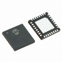
MRF89XA-I/MQ Microchip Technology, MRF89XA-I/MQ Datasheet - Page 73

MRF89XA-I/MQ
Manufacturer Part Number
MRF89XA-I/MQ
Description
TXRX ISM SUB-GHZ ULP 32QFN
Manufacturer
Microchip Technology
Specifications of MRF89XA-I/MQ
Package / Case
32-WFQFN Exposed Pad
Frequency
863MHz ~ 870MHz, 902MHz ~ 928MHz, 950MHz ~ 960MHz
Data Rate - Maximum
200kbps
Modulation Or Protocol
FSK, OOK
Applications
ISM
Power - Output
12.5dBm
Sensitivity
-113dBm
Voltage - Supply
2.1 V ~ 3.6 V
Current - Receiving
3mA
Current - Transmitting
25mA
Data Interface
PCB, Surface Mount
Antenna Connector
PCB, Surface Mount
Operating Temperature
-40°C ~ 85°C
Number Of Receivers
1
Number Of Transmitters
1
Wireless Frequency
863 MHz to 870 MHz, 902 MHz to 928 MHz, 950 MHz to 960 MHz
Interface Type
SPI
Noise Figure
- 112 dBc
Output Power
- 8.5 dBm, + 12.5 dBm
Operating Supply Voltage
2.1 V to 3.6 V
Maximum Operating Temperature
+ 85 C
Mounting Style
SMD/SMT
Maximum Data Rate
256 Kbps
Maximum Supply Current
25 mA
Minimum Operating Temperature
- 40 C
Modulation
FSK
Lead Free Status / RoHS Status
Lead free / RoHS Compliant
Memory Size
-
Lead Free Status / Rohs Status
Lead free / RoHS Compliant
Available stocks
Company
Part Number
Manufacturer
Quantity
Price
Company:
Part Number:
MRF89XA-I/MQ
Manufacturer:
MICROCHIP
Quantity:
12 000
3.4.11
The Bit Synchronizer (BitSync) block provides a clean
and synchronized digital output that is free of glitches.
Figure 3-13 illustrates the BitSync block output when a
Raw Demodulator FSK or OOK output is fed to it.
FIGURE 3-13:
The BitSync can be disabled by setting the BSYNCEN
bit (SYNCREG<6>) to ‘1’ and by holding the IRQ1 pin
(pin 22) low. However, for optimum receiver perfor-
mance, it has to be used when the device is running in
Continuous mode. With this option a DCLK signal is
present on the IRQ1 pin.
The BitSync is automatically activated in Buffered and
Packet modes. The bit synchronizer bit-rate is con-
trolled by the BRVAL<6:0> bits (BRSREG<6:0>). For a
given bit rate, this parameter is determined by
Equation 3-16.
EQUATION 3-16:
For proper operation, the Bit Synchronizer must first
receive three bytes of alternating logic value preamble,
(that is, ‘0101’ sequences). After this start-up phase,
the rising edge of the DCLK signal is centered on the
demodulated bit. Subsequent data transitions will
preserve this centering. This has two implications:
• If the Bit Rates of Transmitter and Receiver are
• If there is a difference in Bit Rate between TX and
© 2010 Microchip Technology Inc.
known to be the same, the MRF89XA will be able
to receive an infinite unbalanced sequence (all
‘0’s or all ‘1’s) with no restriction.
RX, the amount of adjacent bits at the same level
BR
BIT SYNCHRONIZER
=
--------------------------------------------------------------------- -
64 1
•
Continuous mode
To DATA pin and
Raw demodulator
BitSync BLOCK OUTPUT SIGNALS
BitSync Output
+
(FSK or OOK)
[
DCLK in
1
output
+
f
xtal
BRVAL<6:0>
]
DCLK
IRQ1
DATA
Preliminary
EQUATION 3-17:
This implies approximately six consecutive unbalanced
bytes when the Bit Rate precision is 1%, which is easily
achievable (crystal tolerance is or should be at least in
the range of 50 to 100 ppm).
3.4.12
Bit Synchronizer and Active channel filter settings are
a function of the reference oscillator crystal frequency,
f
12.8 MHz crystal can be obtained by selecting the cor-
rect reference oscillator frequency.
xtal
that the BitSync can withstand. It can be esti-
mated as given in Equation 3-17.
. Settings other than those programmable with a
ALTERNATIVE SETTINGS FOR
BITSYNC AND ACTIVE FILTER
NumberOfBits
MRF89XA
=
1
-- -
2
•
---------- -
ΔBR
BR
DS70622B-page 73


