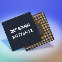
XRT75R12DIB-F Exar Corporation, XRT75R12DIB-F Datasheet - Page 11

XRT75R12DIB-F
Manufacturer Part Number
XRT75R12DIB-F
Description
Peripheral Drivers & Components (PCIs) 12 Channel 3.3V-5V temp -45 to 85C
Manufacturer
Exar Corporation
Datasheet
1.XRT75R12DIB-F.pdf
(133 pages)
Specifications of XRT75R12DIB-F
Maximum Operating Temperature
+ 85 C
Minimum Operating Temperature
- 40 C
Mounting Style
SMD/SMT
Operating Supply Voltage
3.3 V to 5 V
Package / Case
TBGA-420
Lead Free Status / RoHS Status
Lead free / RoHS Compliant
- Current page: 11 of 133
- Download datasheet (851Kb)
SYSTEM-SIDE RECEIVE OUTPUT AND RECEIVE CONTROL PINS
REV. 1.0.3
AC26
AC25
P
AC1
AC2
F23
F24
U23
T24
E24
V23
K24
T23
L23
J23
U4
K3
V4
E3
L4
T3
F3
F4
T4
J4
IN
#
RxNEG/LCV10
RxNEG/LCV11
RxNEG/LCV0
RxNEG/LCV1
RxNEG/LCV2
RxNEG/LCV3
RxNEG/LCV4
RxNEG/LCV5
RxNEG/LCV6
RxNEG/LCV7
RxNEG/LCV8
RxNEG/LCV9
TWELVE CHANNEL E3/DS3/STS-1 LINE INTERFACE UNIT WITH SONET DESYNCHRONIZER
S
RxCLK10
RxCLK11
IGNAL
RxCLK0
RxCLK1
RxCLK2
RxCLK3
RxCLK4
RxCLK5
RxCLK6
RxCLK7
RxCLK8
RxCLK9
N
AME
T
YPE
O
O
Receive Negative Data Output/Line Code Violation
The function of these pins depends on whether the XRT75R12D is configured in
Single Rail or Dual Rail mode.
Dual-Rail Mode - Receive Negative Polarity Data Output
In the Dual-Rail Mode, all negative-polarity data will be output via this pin. The
positive-polarity data will be output via the corresponding RxPOS_n output pin.
In other words, the Receive Section of the corresponding Channel will pulse this
output pin "High" for one period of RxCLK_n anytime it receives a negative-
polarity pulse via the RTIP/RRING input pins.
The data output via this pin is updated upon the active edge of the RCLK_n
output clock signal.
Single-Rail Mode - Line Code Violation Indicator Output
In the Single-Rail Mode, this output pin will function as the Line Code Violation
indicator output.
In this configuration, the Receive Section of the Channel will pulse this output
pin "High" for at least one RCLK period whenever it detects either an LCV (Line
Code Violation) or an EXZ (Excessive Zero Event).
The data that is output via this pin is updated upon the active edge of the
RCLK_n output clock signal.
Receive Clock Output
This output pin functions as the Receive or recovered clock signal. All Receive
(or recovered) data will output via the RxPOS_n and RxNEG_n outputs upon
the active edge of this clock signal.
Additionally, if the device/channel has been configured to operate in the Single-
Rail Mode, then the RNEG_n/LCV_n output pins will also be updated upon the
active edge of this clock signal.
7
D
ESCRIPTION
XRT75R12D
Related parts for XRT75R12DIB-F
Image
Part Number
Description
Manufacturer
Datasheet
Request
R

Part Number:
Description:
Twelve Channel E3/ds3/sts-1 Line Interface Unit With Jitter
Manufacturer:
Exar Corporation
Datasheet:

Part Number:
Description:
BiCMOS Fixed, Quad, Voltage Output, Single or Dual Supply 8-Bit Digital-to-Analog Converter
Manufacturer:
Exar Corporation
Datasheet:

Part Number:
Description:
Manufacturer:
Exar Corporation
Datasheet:

Part Number:
Description:
Voltage-Controlled Oscillator
Manufacturer:
Exar Corporation
Datasheet:

Part Number:
Description:
INTEGRATED LINE TRANSMITTER
Manufacturer:
Exar Corporation
Datasheet:

Part Number:
Description:
Monolithic Function Generator
Manufacturer:
Exar Corporation
Datasheet:

Part Number:
Description:
CMOS Microprocessor Compatible Double-Buffered 12-Bit Digital-to-Analog Converter
Manufacturer:
Exar Corporation
Datasheet:

Part Number:
Description:
CMOS 6 BIT HIGH SPEED ANALOG TO DIGITAL CONVERTER
Manufacturer:
Exar Corporation
Datasheet:

Part Number:
Description:
Manufacturer:
Exar Corporation
Datasheet:

Part Number:
Description:
Manufacturer:
Exar Corporation
Datasheet:

Part Number:
Description:
8-Channel, Voltage Output 10 MHz Input Bandwidth 8-Bit Multiplying DACs with Serial Digital Data Por
Manufacturer:
Exar Corporation
Datasheet:

Part Number:
Description:
15 V CMOS Multiplying10-Bit Digital-to-Analog Converter
Manufacturer:
Exar Corporation
Datasheet:

Part Number:
Description:
Monolithic Function Generator
Manufacturer:
Exar Corporation
Datasheet:


