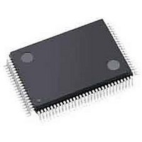
LFXP3C-3TN100I Lattice, LFXP3C-3TN100I Datasheet - Page 223

LFXP3C-3TN100I
Manufacturer Part Number
LFXP3C-3TN100I
Description
FPGA - Field Programmable Gate Array 3.1K LUTs 62 IO 1.8/ 2.5/3.3V -3 Spd I
Manufacturer
Lattice
Specifications of LFXP3C-3TN100I
Number Of Programmable I/os
62
Data Ram Size
55296
Supply Voltage (max)
3.465 V
Maximum Operating Temperature
+ 100 C
Minimum Operating Temperature
- 40 C
Mounting Style
SMD/SMT
Supply Voltage (min)
1.71 V
Package / Case
TQFP-100
Package
100TQFP
Family Name
LatticeXP
Device Logic Units
3000
Maximum Internal Frequency
320 MHz
Typical Operating Supply Voltage
1.8|2.5|3.3 V
Maximum Number Of User I/os
62
Ram Bits
55296
Re-programmability Support
Yes
Lead Free Status / RoHS Status
Lead free / RoHS Compliant
Available stocks
Company
Part Number
Manufacturer
Quantity
Price
Company:
Part Number:
LFXP3C-3TN100I
Manufacturer:
Lattice Semiconductor Corporation
Quantity:
10 000
- Current page: 223 of 397
- Download datasheet (10Mb)
Lattice Semiconductor
Figure 10-4. DQ-DQS Grouping
Figure 10-4 shows a typical DQ-DQS group for both the LatticeECP/EC device and the LatticeXP device. The ninth
I/O of this group of 16 I/Os (for LatticeECP/EC) or 14 I/Os (for LatticeXP) is the dedicated DQS pin. All eight pads
before the DQS and seven (for LatticeECP/EC) or four (for LatticeXP) pads after the DQS are covered by this DQS
bus span. The user can assign any eight of these I/O pads to be DQ data pins. Hence, to implement a 32-bit wide
memory interface you would need to use four such DQ-DQS groups.
When not interfacing with the memory, the dedicated DQS pin can be used as a general purpose I/O. Each of the
dedicated DQS pin is internally connected to the DQS phase shift circuitry. The pinout information contained in the
LatticeECP/EC and LatticeXP device data sheets shows pin locations for the DQS pads. Table 10-2 shows an
extract from the LatticeECP/EC data sheet. In this case, the DQS is marked as LDQS6 (L=left side, 6 =associated
PFU row/column). Since DQS is always the fifth true pad in the DQ-DQS group, counting from low to high PFU
row/column number, LDQS6 will cover PL2A to PL9B. Following this convention, there are eight pads before and
seven pads after DQS for DQ available following counter-clockwise for the left and bottom sides of the device, and
following clockwise for the top and right sides of the device. The user can assign any eight of these pads to be DQ
data signals. The LatticeXP device follows the same method.
Table 10-3. EC20 Pinout (from LatticeECP/EC Family Data Sheet)
Ball Function
PL11A
PL2A
PL2B
PL3A
PL3B
PL4A
PL4B
PL5A
PL5B
PL6A
PL6B
PL7A
PL7B
PL8A
PL8B
PL9A
PL9B
*For LatticeECP/EC: n = 16, for LatticeXP: n = 14.
Bank
7
7
7
7
7
7
7
7
7
7
7
7
7
7
7
7
7
LVDS
C
C
C
C
C
C
C
C
T
T
T
T
T
T
T
T
T
(Ninth I/O Pad)
n* I/O PADS
DQS PAD
10-4
LUM0_PLLC_FB_A
LUM0_PLLT_FB_A
LUM0_PLLC_IN_A
LUM0_PLLT_IN_A
Dual Function
VREF2_7
VREF1_7
LDQS6
—
—
—
—
—
—
—
—
—
—
DQ, DM or VREF1
LatticeECP/EC and LatticeXP
484 fpBGA
G4
G5
D4
E4
C3
B2
E5
D3
C2
E3
D2
B1
C1
E2
F5
F4
F3
DDR Usage Guide
672 fpBGA
G3
G2
G6
H4
G4
E3
E4
B1
C1
F3
D2
E2
D1
E1
F2
F6
J4
Related parts for LFXP3C-3TN100I
Image
Part Number
Description
Manufacturer
Datasheet
Request
R

Part Number:
Description:
FPGA - Field Programmable Gate Array 3.1K LUTs 136 IO 1.8 /2.5/3.3V -3 Spd I
Manufacturer:
Lattice

Part Number:
Description:
FPGA - Field Programmable Gate Array 3.1K LUTs 62 IO 1.8/ 2.5/3.3V -3 Spd I
Manufacturer:
Lattice

Part Number:
Description:
FPGA - Field Programmable Gate Array 3.1K LUTs 136 IO 1.8 /2.5/3.3V -3 Spd
Manufacturer:
Lattice

Part Number:
Description:
FPGA - Field Programmable Gate Array 3.1K LUTs 100 I/O 1.8/2.5/3.3V -3 Spd
Manufacturer:
Lattice
Datasheet:

Part Number:
Description:
FPGA - Field Programmable Gate Array 3.1K LUTS 100 I/O
Manufacturer:
Lattice
Datasheet:

Part Number:
Description:
FPGA - Field Programmable Gate Array 3.1K LUTS 136 I/O
Manufacturer:
Lattice
Datasheet:

Part Number:
Description:
FPGA - Field Programmable Gate Array 3.1K LUTs 100 I/O 1.8/2.5/3.3V -4 Spd
Manufacturer:
Lattice
Datasheet:

Part Number:
Description:
FPGA - Field Programmable Gate Array 3.1K LUTS 62 I/O
Manufacturer:
Lattice
Datasheet:

Part Number:
Description:
FPGA - Field Programmable Gate Array 3.1K LUTs 62 I/O 1.8/2.5/3.3V -4 Spd
Manufacturer:
Lattice
Datasheet:

Part Number:
Description:
FPGA - Field Programmable Gate Array 3.1K LUTS 62 I/O
Manufacturer:
Lattice
Datasheet:

Part Number:
Description:
FPGA - Field Programmable Gate Array 3.1K LUTs 100 I/O 1.8/2.5/3.3V IND
Manufacturer:
Lattice
Datasheet:

Part Number:
Description:
FPGA, 1.8V FLASH, INSTANT ON, SMD
Manufacturer:
LATTICE SEMICONDUCTOR
Datasheet:
Part Number:
Description:
FPGA LatticeXP Family 3000 Cells 320MHz 130nm (CMOS) Technology 1.8V/2.5V/3.3V 208-Pin PQFP Tray
Manufacturer:
LATTICE SEMICONDUCTOR
Datasheet:
Part Number:
Description:
FPGA LatticeXP Family 3000 Cells 320MHz 130nm (CMOS) Technology 1.8V/2.5V/3.3V 144-Pin TQFP Tray
Manufacturer:
LATTICE SEMICONDUCTOR
Datasheet:
Part Number:
Description:
FPGA LatticeXP Family 3000 Cells 360MHz 130nm (CMOS) Technology 1.8V/2.5V/3.3V 100-Pin TQFP Tray
Manufacturer:
LATTICE SEMICONDUCTOR
Datasheet:


