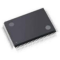
LFXP3C-3TN100I Lattice, LFXP3C-3TN100I Datasheet - Page 334

LFXP3C-3TN100I
Manufacturer Part Number
LFXP3C-3TN100I
Description
FPGA - Field Programmable Gate Array 3.1K LUTs 62 IO 1.8/ 2.5/3.3V -3 Spd I
Manufacturer
Lattice
Specifications of LFXP3C-3TN100I
Number Of Programmable I/os
62
Data Ram Size
55296
Supply Voltage (max)
3.465 V
Maximum Operating Temperature
+ 100 C
Minimum Operating Temperature
- 40 C
Mounting Style
SMD/SMT
Supply Voltage (min)
1.71 V
Package / Case
TQFP-100
Package
100TQFP
Family Name
LatticeXP
Device Logic Units
3000
Maximum Internal Frequency
320 MHz
Typical Operating Supply Voltage
1.8|2.5|3.3 V
Maximum Number Of User I/os
62
Ram Bits
55296
Re-programmability Support
Yes
Lead Free Status / RoHS Status
Lead free / RoHS Compliant
Available stocks
Company
Part Number
Manufacturer
Quantity
Price
Company:
Part Number:
LFXP3C-3TN100I
Manufacturer:
Lattice Semiconductor Corporation
Quantity:
10 000
- Current page: 334 of 397
- Download datasheet (10Mb)
Lattice Semiconductor
beginning of the design cycle. When the pipelining technique is applied, special care must be taken for the rest of
the design to account for the additional data path latency. The following illustrates the same data path before
(Figure 13-5) and after pipelining (Figure 13-6).
Figure 13-5. Before Pipelining
Figure 13-6. After Pipelining
Before pipelining, the clock speed is determined by the clock-to-out time of the source register, the logic delay
through four levels of combinatorial logic, the associated routing delays, and the setup time of the destination regis-
ter. After pipelining is applied, the clock speed is significantly improved by reducing the delay of four logic levels to
one logic level and the associated routing delays, even though the rest of the timing requirements remain the same.
It is recommended to check the Place and Route timing report to ensure that the pipelined design gives the desired
performance.
Comparing IF statement and CASE statement
CASE and IF-THEN-ELSE statements are common for sequential logic in HDL designs. The IF-THEN-ELSE state-
ment generally generates priority-encoded logic, whereas the CASE statement implements balanced logic. An IF-
THEN-ELSE statement can contain a set of different expressions while a Case statement is evaluated against a
common controlling expression. Both statements will give the same functional implementation if the decode condi-
tions are mutually exclusive, as shown in the following VHDL codes.
-- Case Statement — mutually exclusive conditions
process (s, x, y, z)
begin
end process;
O1 <= ‘0’;
O2 <= ‘0’;
O3 <= ‘0’;
case (s) is
end case;
FF1
when “00” => O1 <= x;
when “01” => O2 <= y;
when “10” => O3 <= z;
FF1
Function
Comb.
Function
Comb.
FF2
Slow Clock
Fast Clock
Function
Comb.
13-7
Function
Comb.
-- If-Then-Else — mutually exclusive conditions
process (s, x, y, z)
begin
end process;
O1 <= ‘0’;
O2 <= ‘0’;
O3 <= ‘0’;
if s = “00” then O1 <= x;
elsif s = “01” then O2 <= y;
elsif s = “10” then O3 <= z;
end if;
Function
Comb.
HDL Synthesis Coding Guidelines
for Lattice Semiconductor FPGAs
FF3
Function
FF1
Comb.
FF4
Related parts for LFXP3C-3TN100I
Image
Part Number
Description
Manufacturer
Datasheet
Request
R

Part Number:
Description:
FPGA - Field Programmable Gate Array 3.1K LUTs 136 IO 1.8 /2.5/3.3V -3 Spd I
Manufacturer:
Lattice

Part Number:
Description:
FPGA - Field Programmable Gate Array 3.1K LUTs 62 IO 1.8/ 2.5/3.3V -3 Spd I
Manufacturer:
Lattice

Part Number:
Description:
FPGA - Field Programmable Gate Array 3.1K LUTs 136 IO 1.8 /2.5/3.3V -3 Spd
Manufacturer:
Lattice

Part Number:
Description:
FPGA - Field Programmable Gate Array 3.1K LUTs 100 I/O 1.8/2.5/3.3V -3 Spd
Manufacturer:
Lattice
Datasheet:

Part Number:
Description:
FPGA - Field Programmable Gate Array 3.1K LUTS 100 I/O
Manufacturer:
Lattice
Datasheet:

Part Number:
Description:
FPGA - Field Programmable Gate Array 3.1K LUTS 136 I/O
Manufacturer:
Lattice
Datasheet:

Part Number:
Description:
FPGA - Field Programmable Gate Array 3.1K LUTs 100 I/O 1.8/2.5/3.3V -4 Spd
Manufacturer:
Lattice
Datasheet:

Part Number:
Description:
FPGA - Field Programmable Gate Array 3.1K LUTS 62 I/O
Manufacturer:
Lattice
Datasheet:

Part Number:
Description:
FPGA - Field Programmable Gate Array 3.1K LUTs 62 I/O 1.8/2.5/3.3V -4 Spd
Manufacturer:
Lattice
Datasheet:

Part Number:
Description:
FPGA - Field Programmable Gate Array 3.1K LUTS 62 I/O
Manufacturer:
Lattice
Datasheet:

Part Number:
Description:
FPGA - Field Programmable Gate Array 3.1K LUTs 100 I/O 1.8/2.5/3.3V IND
Manufacturer:
Lattice
Datasheet:

Part Number:
Description:
FPGA, 1.8V FLASH, INSTANT ON, SMD
Manufacturer:
LATTICE SEMICONDUCTOR
Datasheet:
Part Number:
Description:
FPGA LatticeXP Family 3000 Cells 320MHz 130nm (CMOS) Technology 1.8V/2.5V/3.3V 208-Pin PQFP Tray
Manufacturer:
LATTICE SEMICONDUCTOR
Datasheet:
Part Number:
Description:
FPGA LatticeXP Family 3000 Cells 320MHz 130nm (CMOS) Technology 1.8V/2.5V/3.3V 144-Pin TQFP Tray
Manufacturer:
LATTICE SEMICONDUCTOR
Datasheet:
Part Number:
Description:
FPGA LatticeXP Family 3000 Cells 360MHz 130nm (CMOS) Technology 1.8V/2.5V/3.3V 100-Pin TQFP Tray
Manufacturer:
LATTICE SEMICONDUCTOR
Datasheet:


