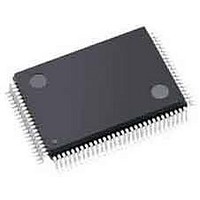
LFXP3C-3TN100I Lattice, LFXP3C-3TN100I Datasheet - Page 302

LFXP3C-3TN100I
Manufacturer Part Number
LFXP3C-3TN100I
Description
FPGA - Field Programmable Gate Array 3.1K LUTs 62 IO 1.8/ 2.5/3.3V -3 Spd I
Manufacturer
Lattice
Specifications of LFXP3C-3TN100I
Number Of Programmable I/os
62
Data Ram Size
55296
Supply Voltage (max)
3.465 V
Maximum Operating Temperature
+ 100 C
Minimum Operating Temperature
- 40 C
Mounting Style
SMD/SMT
Supply Voltage (min)
1.71 V
Package / Case
TQFP-100
Package
100TQFP
Family Name
LatticeXP
Device Logic Units
3000
Maximum Internal Frequency
320 MHz
Typical Operating Supply Voltage
1.8|2.5|3.3 V
Maximum Number Of User I/os
62
Ram Bits
55296
Re-programmability Support
Yes
Lead Free Status / RoHS Status
Lead free / RoHS Compliant
Available stocks
Company
Part Number
Manufacturer
Quantity
Price
Company:
Part Number:
LFXP3C-3TN100I
Manufacturer:
Lattice Semiconductor Corporation
Quantity:
10 000
- Current page: 302 of 397
- Download datasheet (10Mb)
Lattice Semiconductor
Dedicated Pins
Following is a description of the dedicated sysCONFIG pins for the LatticeXP device. These pins are used to con-
trol or monitor the configuration process. These pins are used for non-JTAG programming sequences only. The
JTAG pins will be explained later in the ispJTAG Pins section of this document.
CFG[1:0]
The Configuration Mode pins, CFG[1:0], are dedicated inputs with weak pull-ups. The CFG pins are used to select
the configuration mode for the LatticeXP, i.e. what type of device the LatticeXP will configure from. At Power-On-
Reset (POR), or when the PROGRAMN pin is driven low, and depending on the configuration mode selected, dif-
ferent groups of dual-purpose pins will be used for device configuration.
Table 13-2. LatticeXP Configuration Modes
When both CFG pins are high the device will configure itself by reading the data stored in on-chip Flash; this is
referred to as SDM, or Self Download Mode. See the Self-Download section of this document for more information
regarding SDM.
PROGRAMN
The PROGRAMN pin is a dedicated input with a weak pull-up. This pin is used to initiate a non-JTAG SRAM config-
uration sequence. A high to low signal applied to PROGRAMN sets the device into configuration mode. The PRO-
GRAMN pin can be used to trigger configuration at any time. If the device is using JTAG then PROGRAMN will be
ignored until the device is released from JTAG mode.
PROGRAMN should not be low externally during power-up. It should be driven high or rising with the power supply
via an external pullup resistor. Once all power supplies have reached minimum levels, PROGRAMN may be used
to initiate the configuration process.
If the CFG pins are not both high (not in SDM) then the configuration sequence will proceed using the selected
configuration port. If both CFG pins are high (SDM), and the Flash has been programmed, then the configuration
sequence will proceed using the data in on-chip Flash.
If both CFG pins are high (SDM), and the Flash has not been programmed, the configuration sequence will pause
and wait for the Flash done bit to be programmed. Once the Flash has been programmed, and PROGRAMN is
brought high, the configuration sequence will continue.
INITN
The INITN pin is a dedicated bi-directional open drain pin with a weak pull-up. INITN is capable of driving a low
pulse out as well as detecting a low pulse driven in.
Table 13-1. Configuration Pins for the LatticeXP Device (Continued)
TDO
TCK
TMS
Note: Weak pull-ups consist of a current source of 30uA to 150uA. The pull-ups for CFG and PROGRAMN track V
TDI and TMS track V
Pin Name
Output
Input with Hysteresis
Input, weak pull-up
CCJ
; all other pull-ups track the V
Slave Serial
Master Serial
Slave Parallel
Self Download Mode (SDM)
Configuration Mode
I/O Type
CCIO
for that pin.
13-3
CFG[1]
0
0
1
1
LatticeXP sysCONFIG Usage Guide
CFG[0]
0
0
1
1
Pin Type
JTAG
JTAG
JTAG
CC
(core); the pull-ups for
Mode Used
Related parts for LFXP3C-3TN100I
Image
Part Number
Description
Manufacturer
Datasheet
Request
R

Part Number:
Description:
FPGA - Field Programmable Gate Array 3.1K LUTs 136 IO 1.8 /2.5/3.3V -3 Spd I
Manufacturer:
Lattice

Part Number:
Description:
FPGA - Field Programmable Gate Array 3.1K LUTs 62 IO 1.8/ 2.5/3.3V -3 Spd I
Manufacturer:
Lattice

Part Number:
Description:
FPGA - Field Programmable Gate Array 3.1K LUTs 136 IO 1.8 /2.5/3.3V -3 Spd
Manufacturer:
Lattice

Part Number:
Description:
FPGA - Field Programmable Gate Array 3.1K LUTs 100 I/O 1.8/2.5/3.3V -3 Spd
Manufacturer:
Lattice
Datasheet:

Part Number:
Description:
FPGA - Field Programmable Gate Array 3.1K LUTS 100 I/O
Manufacturer:
Lattice
Datasheet:

Part Number:
Description:
FPGA - Field Programmable Gate Array 3.1K LUTS 136 I/O
Manufacturer:
Lattice
Datasheet:

Part Number:
Description:
FPGA - Field Programmable Gate Array 3.1K LUTs 100 I/O 1.8/2.5/3.3V -4 Spd
Manufacturer:
Lattice
Datasheet:

Part Number:
Description:
FPGA - Field Programmable Gate Array 3.1K LUTS 62 I/O
Manufacturer:
Lattice
Datasheet:

Part Number:
Description:
FPGA - Field Programmable Gate Array 3.1K LUTs 62 I/O 1.8/2.5/3.3V -4 Spd
Manufacturer:
Lattice
Datasheet:

Part Number:
Description:
FPGA - Field Programmable Gate Array 3.1K LUTS 62 I/O
Manufacturer:
Lattice
Datasheet:

Part Number:
Description:
FPGA - Field Programmable Gate Array 3.1K LUTs 100 I/O 1.8/2.5/3.3V IND
Manufacturer:
Lattice
Datasheet:

Part Number:
Description:
FPGA, 1.8V FLASH, INSTANT ON, SMD
Manufacturer:
LATTICE SEMICONDUCTOR
Datasheet:
Part Number:
Description:
FPGA LatticeXP Family 3000 Cells 320MHz 130nm (CMOS) Technology 1.8V/2.5V/3.3V 208-Pin PQFP Tray
Manufacturer:
LATTICE SEMICONDUCTOR
Datasheet:
Part Number:
Description:
FPGA LatticeXP Family 3000 Cells 320MHz 130nm (CMOS) Technology 1.8V/2.5V/3.3V 144-Pin TQFP Tray
Manufacturer:
LATTICE SEMICONDUCTOR
Datasheet:
Part Number:
Description:
FPGA LatticeXP Family 3000 Cells 360MHz 130nm (CMOS) Technology 1.8V/2.5V/3.3V 100-Pin TQFP Tray
Manufacturer:
LATTICE SEMICONDUCTOR
Datasheet:


