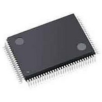
LFXP3C-3TN100I Lattice, LFXP3C-3TN100I Datasheet - Page 235

LFXP3C-3TN100I
Manufacturer Part Number
LFXP3C-3TN100I
Description
FPGA - Field Programmable Gate Array 3.1K LUTs 62 IO 1.8/ 2.5/3.3V -3 Spd I
Manufacturer
Lattice
Specifications of LFXP3C-3TN100I
Number Of Programmable I/os
62
Data Ram Size
55296
Supply Voltage (max)
3.465 V
Maximum Operating Temperature
+ 100 C
Minimum Operating Temperature
- 40 C
Mounting Style
SMD/SMT
Supply Voltage (min)
1.71 V
Package / Case
TQFP-100
Package
100TQFP
Family Name
LatticeXP
Device Logic Units
3000
Maximum Internal Frequency
320 MHz
Typical Operating Supply Voltage
1.8|2.5|3.3 V
Maximum Number Of User I/os
62
Ram Bits
55296
Re-programmability Support
Yes
Lead Free Status / RoHS Status
Lead free / RoHS Compliant
Available stocks
Company
Part Number
Manufacturer
Quantity
Price
Company:
Part Number:
LFXP3C-3TN100I
Manufacturer:
Lattice Semiconductor Corporation
Quantity:
10 000
- Current page: 235 of 397
- Download datasheet (10Mb)
Lattice Semiconductor
Write Timing Waveforms
Figure 10-17 shows DDR write side data transfer timing for the DQ Data pad and the DQS Strobe Pad. When writ-
ing to the DDR memory device, the DM (Data Mask) and the ADDR/ CMD (Address and Command) signals are
also sent to the memory device along with the data and strobe signals.
Figure 10-17. DDR Write Data Transfer for DQ Data
Design Rules/Guidelines
Listed below are some rules and guidelines to keep in mind when implementing DDR memory interfaces in the Lat-
ticeECP/EC and LatticeXP devices.
• The LatticeECP/EC and LatticeXP devices have dedicated DQ-DQS banks. Please refer to the logical sig-
• There are two DQSDLLs on the device, one for the top half and one for the bottom half. Hence, only one
nal connections of the groups in the LatticeECP/EC and LatticeXP data sheets before locking these pins.
DQSDLL primitive should be instantiated for each half of the device. Since there is only one DQSDLL on
each half of the device, all the DDR memory interfaces on that half of the device should run at the same fre-
quency. Each DQSDLL will generate 90 degree digital delay bits for all the DQS delay blocks on that half of
the device based on the reference clock input to the DLL.
DATAOUT_N
DATAOUT_P
CLK +270
CLK +180
CLKP
CLKN
CLK
DQS
DQ
Notes -
(1) DATAOUT_P and DATAOUT_N are inputs to the DDR output registers.
(2) DQS is generated at 270 degree phase of CLK.
(3) CLKP is generated simular to DQS and CLKN is the inverted CLKP.
(4) DQ is generated at 180 degree phase of CLK.
(5) DQ is center aligned with the DQS strobe signal when it reaches the memory.
P0
N0
P0
N0
10-16
P1
N1
P1
N1
P2
N2
LatticeECP/EC and LatticeXP
P2
N2
DDR Usage Guide
Related parts for LFXP3C-3TN100I
Image
Part Number
Description
Manufacturer
Datasheet
Request
R

Part Number:
Description:
FPGA - Field Programmable Gate Array 3.1K LUTs 136 IO 1.8 /2.5/3.3V -3 Spd I
Manufacturer:
Lattice

Part Number:
Description:
FPGA - Field Programmable Gate Array 3.1K LUTs 62 IO 1.8/ 2.5/3.3V -3 Spd I
Manufacturer:
Lattice

Part Number:
Description:
FPGA - Field Programmable Gate Array 3.1K LUTs 136 IO 1.8 /2.5/3.3V -3 Spd
Manufacturer:
Lattice

Part Number:
Description:
FPGA - Field Programmable Gate Array 3.1K LUTs 100 I/O 1.8/2.5/3.3V -3 Spd
Manufacturer:
Lattice
Datasheet:

Part Number:
Description:
FPGA - Field Programmable Gate Array 3.1K LUTS 100 I/O
Manufacturer:
Lattice
Datasheet:

Part Number:
Description:
FPGA - Field Programmable Gate Array 3.1K LUTS 136 I/O
Manufacturer:
Lattice
Datasheet:

Part Number:
Description:
FPGA - Field Programmable Gate Array 3.1K LUTs 100 I/O 1.8/2.5/3.3V -4 Spd
Manufacturer:
Lattice
Datasheet:

Part Number:
Description:
FPGA - Field Programmable Gate Array 3.1K LUTS 62 I/O
Manufacturer:
Lattice
Datasheet:

Part Number:
Description:
FPGA - Field Programmable Gate Array 3.1K LUTs 62 I/O 1.8/2.5/3.3V -4 Spd
Manufacturer:
Lattice
Datasheet:

Part Number:
Description:
FPGA - Field Programmable Gate Array 3.1K LUTS 62 I/O
Manufacturer:
Lattice
Datasheet:

Part Number:
Description:
FPGA - Field Programmable Gate Array 3.1K LUTs 100 I/O 1.8/2.5/3.3V IND
Manufacturer:
Lattice
Datasheet:

Part Number:
Description:
FPGA, 1.8V FLASH, INSTANT ON, SMD
Manufacturer:
LATTICE SEMICONDUCTOR
Datasheet:
Part Number:
Description:
FPGA LatticeXP Family 3000 Cells 320MHz 130nm (CMOS) Technology 1.8V/2.5V/3.3V 208-Pin PQFP Tray
Manufacturer:
LATTICE SEMICONDUCTOR
Datasheet:
Part Number:
Description:
FPGA LatticeXP Family 3000 Cells 320MHz 130nm (CMOS) Technology 1.8V/2.5V/3.3V 144-Pin TQFP Tray
Manufacturer:
LATTICE SEMICONDUCTOR
Datasheet:
Part Number:
Description:
FPGA LatticeXP Family 3000 Cells 360MHz 130nm (CMOS) Technology 1.8V/2.5V/3.3V 100-Pin TQFP Tray
Manufacturer:
LATTICE SEMICONDUCTOR
Datasheet:


