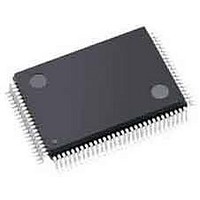
LFXP3C-3TN100I Lattice, LFXP3C-3TN100I Datasheet - Page 371

LFXP3C-3TN100I
Manufacturer Part Number
LFXP3C-3TN100I
Description
FPGA - Field Programmable Gate Array 3.1K LUTs 62 IO 1.8/ 2.5/3.3V -3 Spd I
Manufacturer
Lattice
Specifications of LFXP3C-3TN100I
Number Of Programmable I/os
62
Data Ram Size
55296
Supply Voltage (max)
3.465 V
Maximum Operating Temperature
+ 100 C
Minimum Operating Temperature
- 40 C
Mounting Style
SMD/SMT
Supply Voltage (min)
1.71 V
Package / Case
TQFP-100
Package
100TQFP
Family Name
LatticeXP
Device Logic Units
3000
Maximum Internal Frequency
320 MHz
Typical Operating Supply Voltage
1.8|2.5|3.3 V
Maximum Number Of User I/os
62
Ram Bits
55296
Re-programmability Support
Yes
Lead Free Status / RoHS Status
Lead free / RoHS Compliant
Available stocks
Company
Part Number
Manufacturer
Quantity
Price
Company:
Part Number:
LFXP3C-3TN100I
Manufacturer:
Lattice Semiconductor Corporation
Quantity:
10 000
- Current page: 371 of 397
- Download datasheet (10Mb)
Lattice Semiconductor
IN_DEL
ROUTE
NCLK_DEL
ROUTE
NCLK_DEL
ROUTE
Report: There is no minimum offset greater than zero for this preference.
From the Set-up Report below, which was run for MAX conditions:
===========================================================================
Preference: CLOCK_TO_OUT PORT “ddr_cas_n” MAX 5.500000 ns CLKPORT “clk” CLKOUT PORT “ddr_clk”
;
---------------------------------------------------------------------------------------------
------------------------------------
Passed:
ddr_clk_c -)
Logical Details:
Constraint Details:
Physical Path Details:
Name
Name
Source:
Destination:
Data Path Delay:
Clock Path Delay:
•
Clock path clk to ddr_dq_31:
Feedback path:
t
6.346ns delay clk to ddr_cas_n less
3.271ns feedback compensation
1.713ns delay ddr_cas_n to ddr_cas_n less
2.470ns delay clk to ddr_clk (totaling 2.318ns) meets
5.500ns offset clk to ddr_cas_n by 3.182ns
Clock path clk to ddr_cas_n:
DDR_CLK
The following path meets requirements by 3.182ns
Fanout
Fanout
---
---
136
---
136
1 item scored, 0 timing errors detected.
(max) = 5.741 - 3.271 = 2.47 ns
1
--------
--------
Unknown
Cell type
Port
Delay (ns)
0.576
0.507
0.231
1.830
3.144
Delay (ns)
0.231
1.674
1.905
1.713ns
6.346ns
LLHPPLL.CLKIN to
LLHPPLL.CLKIN to
LLHPPLL.NCLK to
(25.7% logic, 74.3% route), 2 logic levels.
LLHPPLL.NCLK to
(12.1% logic, 87.9% route), 1 logic levels.
Q
Pin type
Pad
AB4.INCK to
AB4.PAD to
(100.0% logic, 0.0% route), 1 logic levels.
(28.6% logic, 71.4% route), 2 logic levels.
Site
Site
18-11
U1_ddrct_np_o4_1_008/U1_cmdexe/ddr_cas_nZ0
LLHPPLL.CLKIN clk_c
Cell name
ddr_cas_n
LLHPPLL.NCLK U2_ddr_pll_orca/ddr_pll_0_0
LLHPPLL.NCLK U2_ddr_pll_orca/ddr_pll_0_0
LLHPPLL.FB pll_nclk
AB4.INCK clk
C25.SC pll_nclk
for the DDR SDRAM Controller IP Core
(clock net +/-)
Resource
Resource
Board Timing Guidelines
(from
Related parts for LFXP3C-3TN100I
Image
Part Number
Description
Manufacturer
Datasheet
Request
R

Part Number:
Description:
FPGA - Field Programmable Gate Array 3.1K LUTs 136 IO 1.8 /2.5/3.3V -3 Spd I
Manufacturer:
Lattice

Part Number:
Description:
FPGA - Field Programmable Gate Array 3.1K LUTs 62 IO 1.8/ 2.5/3.3V -3 Spd I
Manufacturer:
Lattice

Part Number:
Description:
FPGA - Field Programmable Gate Array 3.1K LUTs 136 IO 1.8 /2.5/3.3V -3 Spd
Manufacturer:
Lattice

Part Number:
Description:
FPGA - Field Programmable Gate Array 3.1K LUTs 100 I/O 1.8/2.5/3.3V -3 Spd
Manufacturer:
Lattice
Datasheet:

Part Number:
Description:
FPGA - Field Programmable Gate Array 3.1K LUTS 100 I/O
Manufacturer:
Lattice
Datasheet:

Part Number:
Description:
FPGA - Field Programmable Gate Array 3.1K LUTS 136 I/O
Manufacturer:
Lattice
Datasheet:

Part Number:
Description:
FPGA - Field Programmable Gate Array 3.1K LUTs 100 I/O 1.8/2.5/3.3V -4 Spd
Manufacturer:
Lattice
Datasheet:

Part Number:
Description:
FPGA - Field Programmable Gate Array 3.1K LUTS 62 I/O
Manufacturer:
Lattice
Datasheet:

Part Number:
Description:
FPGA - Field Programmable Gate Array 3.1K LUTs 62 I/O 1.8/2.5/3.3V -4 Spd
Manufacturer:
Lattice
Datasheet:

Part Number:
Description:
FPGA - Field Programmable Gate Array 3.1K LUTS 62 I/O
Manufacturer:
Lattice
Datasheet:

Part Number:
Description:
FPGA - Field Programmable Gate Array 3.1K LUTs 100 I/O 1.8/2.5/3.3V IND
Manufacturer:
Lattice
Datasheet:

Part Number:
Description:
FPGA, 1.8V FLASH, INSTANT ON, SMD
Manufacturer:
LATTICE SEMICONDUCTOR
Datasheet:
Part Number:
Description:
FPGA LatticeXP Family 3000 Cells 320MHz 130nm (CMOS) Technology 1.8V/2.5V/3.3V 208-Pin PQFP Tray
Manufacturer:
LATTICE SEMICONDUCTOR
Datasheet:
Part Number:
Description:
FPGA LatticeXP Family 3000 Cells 320MHz 130nm (CMOS) Technology 1.8V/2.5V/3.3V 144-Pin TQFP Tray
Manufacturer:
LATTICE SEMICONDUCTOR
Datasheet:
Part Number:
Description:
FPGA LatticeXP Family 3000 Cells 360MHz 130nm (CMOS) Technology 1.8V/2.5V/3.3V 100-Pin TQFP Tray
Manufacturer:
LATTICE SEMICONDUCTOR
Datasheet:


