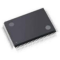
LFXP3C-3TN100I Lattice, LFXP3C-3TN100I Datasheet - Page 225

LFXP3C-3TN100I
Manufacturer Part Number
LFXP3C-3TN100I
Description
FPGA - Field Programmable Gate Array 3.1K LUTs 62 IO 1.8/ 2.5/3.3V -3 Spd I
Manufacturer
Lattice
Specifications of LFXP3C-3TN100I
Number Of Programmable I/os
62
Data Ram Size
55296
Supply Voltage (max)
3.465 V
Maximum Operating Temperature
+ 100 C
Minimum Operating Temperature
- 40 C
Mounting Style
SMD/SMT
Supply Voltage (min)
1.71 V
Package / Case
TQFP-100
Package
100TQFP
Family Name
LatticeXP
Device Logic Units
3000
Maximum Internal Frequency
320 MHz
Typical Operating Supply Voltage
1.8|2.5|3.3 V
Maximum Number Of User I/os
62
Ram Bits
55296
Re-programmability Support
Yes
Lead Free Status / RoHS Status
Lead free / RoHS Compliant
Available stocks
Company
Part Number
Manufacturer
Quantity
Price
Company:
Part Number:
LFXP3C-3TN100I
Manufacturer:
Lattice Semiconductor Corporation
Quantity:
10 000
- Current page: 225 of 397
- Download datasheet (10Mb)
Lattice Semiconductor
The DLL Lock Detect circuit has two modes of operation controlled by the LOCK_SENSITIVITY bit, which selects
more or less sensitivity to jitter. If this DLL is operated at or above 150 MHz, it is recommended that the
LOCK_SENSITIVITY bit be programmed “HIGH” (more sensitive). For operation running at or under 100 MHz it is
recommended that the bit be programmed “LOW” (more tolerant). For 133 MHz, the LOCK_SENSITIVITY bit can
go either way.
DQSBUF
This primitive implements the DQS Delay and the DQS transition detector logic. Figure 10-6 shows the DQSBUFB
function. The preamble detect signal is also generated within this primitive.
Figure 10-6. DQSBUFB Function
Figure 10-7 shows the primitive symbol and its ports. DQSI is the DQS signal from the memory. PRMBDET is the
preamble detect signal that is generated from the DQSI input. READ and CLK are user interface signals coming
from the FPGA logic. The DQSDLL block sends digital control line DQSDEL to this block. The DQS is delayed
based on this input from the DQSDLL. DQSO is the delayed DQS and is connected to the clock input of the first set
of DDR registers.
Figure 10-7. DQSBUFB Symbol
Table 10-5 provides a description of the I/O ports associated with the DQSBUFB primitive.
READ
DQSI
CLK
V
(DV ~ 170mV)
REF
V
REF
- DV
+
-
+
-
PRMBDET
DQSI
CLK
READ
DQSDEL
DQSBUFB
DQSBUFB
10-6
DDRCLKPOL
TRANSITION
PRMBDET
DQSDEL
DETECT
DQS
DQSO
DQSC
DQSDEL
LatticeECP/EC and LatticeXP
DQSC
PRMBDET
DDRCLKPOL
DQSO
DDR Usage Guide
Related parts for LFXP3C-3TN100I
Image
Part Number
Description
Manufacturer
Datasheet
Request
R

Part Number:
Description:
FPGA - Field Programmable Gate Array 3.1K LUTs 136 IO 1.8 /2.5/3.3V -3 Spd I
Manufacturer:
Lattice

Part Number:
Description:
FPGA - Field Programmable Gate Array 3.1K LUTs 62 IO 1.8/ 2.5/3.3V -3 Spd I
Manufacturer:
Lattice

Part Number:
Description:
FPGA - Field Programmable Gate Array 3.1K LUTs 136 IO 1.8 /2.5/3.3V -3 Spd
Manufacturer:
Lattice

Part Number:
Description:
FPGA - Field Programmable Gate Array 3.1K LUTs 100 I/O 1.8/2.5/3.3V -3 Spd
Manufacturer:
Lattice
Datasheet:

Part Number:
Description:
FPGA - Field Programmable Gate Array 3.1K LUTS 100 I/O
Manufacturer:
Lattice
Datasheet:

Part Number:
Description:
FPGA - Field Programmable Gate Array 3.1K LUTS 136 I/O
Manufacturer:
Lattice
Datasheet:

Part Number:
Description:
FPGA - Field Programmable Gate Array 3.1K LUTs 100 I/O 1.8/2.5/3.3V -4 Spd
Manufacturer:
Lattice
Datasheet:

Part Number:
Description:
FPGA - Field Programmable Gate Array 3.1K LUTS 62 I/O
Manufacturer:
Lattice
Datasheet:

Part Number:
Description:
FPGA - Field Programmable Gate Array 3.1K LUTs 62 I/O 1.8/2.5/3.3V -4 Spd
Manufacturer:
Lattice
Datasheet:

Part Number:
Description:
FPGA - Field Programmable Gate Array 3.1K LUTS 62 I/O
Manufacturer:
Lattice
Datasheet:

Part Number:
Description:
FPGA - Field Programmable Gate Array 3.1K LUTs 100 I/O 1.8/2.5/3.3V IND
Manufacturer:
Lattice
Datasheet:

Part Number:
Description:
FPGA, 1.8V FLASH, INSTANT ON, SMD
Manufacturer:
LATTICE SEMICONDUCTOR
Datasheet:
Part Number:
Description:
FPGA LatticeXP Family 3000 Cells 320MHz 130nm (CMOS) Technology 1.8V/2.5V/3.3V 208-Pin PQFP Tray
Manufacturer:
LATTICE SEMICONDUCTOR
Datasheet:
Part Number:
Description:
FPGA LatticeXP Family 3000 Cells 320MHz 130nm (CMOS) Technology 1.8V/2.5V/3.3V 144-Pin TQFP Tray
Manufacturer:
LATTICE SEMICONDUCTOR
Datasheet:
Part Number:
Description:
FPGA LatticeXP Family 3000 Cells 360MHz 130nm (CMOS) Technology 1.8V/2.5V/3.3V 100-Pin TQFP Tray
Manufacturer:
LATTICE SEMICONDUCTOR
Datasheet:


