PIC32MX695F512L-80I/BG Microchip Technology, PIC32MX695F512L-80I/BG Datasheet - Page 129
PIC32MX695F512L-80I/BG
Manufacturer Part Number
PIC32MX695F512L-80I/BG
Description
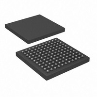
IC, 32BIT MCU, PIC32, 80MHZ, BGA-100
Manufacturer
Microchip Technology
Series
PIC® 32MXr
Datasheets
1.PIC32MX320F032H-40IPT.pdf
(66 pages)
2.PIC32MX575F256H-80IMR.pdf
(2 pages)
3.PIC32MX575F256H-80IMR.pdf
(254 pages)
4.PIC32MX575F256H-80IMR.pdf
(14 pages)
5.PIC32MX575F256H-80IPT.pdf
(240 pages)
Specifications of PIC32MX695F512L-80I/BG
Controller Family/series
PIC32
Ram Memory Size
128KB
Cpu Speed
80MHz
No. Of Timers
5
Interface
I2C, SPI, UART, USB
No. Of Pwm Channels
5
Core Size
32 Bit
Program Memory Size
512 KB
Core Processor
MIPS32® M4K™
Speed
80MHz
Connectivity
Ethernet, I²C, SPI, UART/USART, USB OTG
Peripherals
Brown-out Detect/Reset, DMA, POR, PWM, WDT
Program Memory Type
FLASH
Ram Size
128K x 8
Voltage - Supply (vcc/vdd)
2.3 V ~ 3.6 V
Data Converters
A/D 16x10b
Oscillator Type
Internal
Operating Temperature
-40°C ~ 85°C
Package / Case
121-TFBGA
Embedded Interface Type
I2C, SPI, UART, USB
Rohs Compliant
Yes
Processor Series
PIC32MX6xx
Core
MIPS
3rd Party Development Tools
52713-733, 52714-737
Development Tools By Supplier
PG164130, DV164035, DV244005
Lead Free Status / RoHS Status
Lead free / RoHS Compliant
Number Of I /o
-
Eeprom Size
-
Lead Free Status / Rohs Status
Details
Available stocks
Company
Part Number
Manufacturer
Quantity
Price
Company:

Part Number:
PIC32MX695F512L-80I/BG
Manufacturer:
Microchip Technology
Quantity:
135
Company:
Part Number:
PIC32MX695F512L-80I/BG
Manufacturer:
Microchip Technology
Quantity:
10 000


16.0
FIGURE 16-1:
2009 Microchip Technology Inc.
Note 1: This data sheet summarizes the features
Note 1: Where ‘x’ is shown, reference is made to the registers associated with the respective output compare channels
2: Some registers and associated bits
OUTPUT COMPARE
2: The OCFA pin controls the OC1-OC4 channels. The OCFB pin controls the OC5 channel.
3: Each output compare channel can use one of two selectable 16-bit time bases or a single 32-bit timer base.
of the PIC32MX5XX/6XX/7XX family of
devices. It is not intended to be a
comprehensive reference source. To
complement the information in this data
sheet, refer to Section 16. “Output
Capture”
Family Reference Manual” , which is
available from the Microchip web site
(www.microchip.com/PIC32).
described in this section may not be avail-
able on all devices. Refer to Section 4.0
“Memory Organization” in this data
sheet for device-specific register and bit
information.
1 through 5.
16
TMR register inputs
from time bases
(see Note 3).
OUTPUT COMPARE MODULE BLOCK DIAGRAM
Comparator
OCxRS
0
OCxR
(DS61111) in the “PIC32MX
(1)
(1)
1
16
OCTSEL
Period match signals
from time bases
(see Note 3).
0
Preliminary
1
PIC32MX5XX/6XX/7XX
Mode Select
OCM<2:0>
The Output Compare module (OCMP) is used to gen-
erate a single pulse or a train of pulses in response to
selected time base events. For all modes of operation,
the OCMP module compares the values stored in the
OCxR and/or the OCxRS registers to the value in the
selected timer. When a match occurs, the OCMP mod-
ule generates an event based on the selected mode of
operation.
The following are some of the key features:
• Multiple Output Compare Modules in a Device
• Programmable Interrupt Generation on Compare
• Single and Dual Compare modes
• Single and Continuous Output Pulse Generation
• Pulse-Width Modulation (PWM) mode
• Hardware-based PWM Fault Detection and
• Programmable Selection of 16-bit or 32-bit Time
• Can Operate from Either of Two Available 16-bit
Event
Automatic Output Disable
Bases.
Time Bases or a Single 32-bit Time Base.
Output
3
Logic
Set Flag bit
OCxIF
(1)
R
S
Q
Output Enable
DS61156B-page 129
OCFA or OCFB
(see Note 2)
OCx
(1)
Related parts for PIC32MX695F512L-80I/BG
Image
Part Number
Description
Manufacturer
Datasheet
Request
R

Part Number:
Description:
Manufacturer:
Microchip Technology Inc.
Datasheet:
Part Number:
Description:
Manufacturer:
Microchip Technology Inc.
Datasheet:
Part Number:
Description:
Manufacturer:
Microchip Technology Inc.
Datasheet:
Part Number:
Description:
Manufacturer:
Microchip Technology Inc.
Datasheet:
Part Number:
Description:
Manufacturer:
Microchip Technology Inc.
Datasheet:
Part Number:
Description:
Manufacturer:
Microchip Technology Inc.
Datasheet:
Part Number:
Description:
Manufacturer:
Microchip Technology Inc.
Datasheet:
Part Number:
Description:
Manufacturer:
Microchip Technology Inc.
Datasheet: