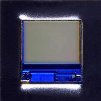
MT9V011P11STC:B Aptina LLC, MT9V011P11STC:B Datasheet - Page 18

MT9V011P11STC:B
Manufacturer Part Number
MT9V011P11STC:B
Description
SENSOR IMAGE VGA COLOR CMOS PLCC
Manufacturer
Aptina LLC
Series
DigitalClarity®, Micron®r
Type
CMOS Imagingr
Datasheets
1.MT9V011P11STCB.pdf
(33 pages)
2.MT9V011P11STCB.pdf
(2 pages)
3.MT9V011P11STCB.pdf
(2 pages)
Specifications of MT9V011P11STC:B
Pixel Size
5.6µm x 5.6µm
Active Pixel Array
640H x 480V
Frames Per Second
30
Voltage - Supply
2.8V
Package / Case
28-PLCC
Lead Free Status / RoHS Status
Lead free / RoHS Compliant
Other names
557-1315
Available stocks
Company
Part Number
Manufacturer
Quantity
Price
Company:
Part Number:
MT9V011P11STC:B
Manufacturer:
RENESAS
Quantity:
1 001
Part Number:
MT9V011P11STC:B
Manufacturer:
MICRON
Quantity:
20 000
Table 7:
PDF: 817d5189/Source: 817d5173
MT9V011_C82S_2_PLCC.fm - Rev. B 1/05 EN
Register
Pixel Integration Control
These registers (along with the Window Size and Blanking registers) control the integration time for the pixels.
Pixel Clock Speed
Frame Restart
Reset (Soft)
Zoom Mode / True Decimation Mode
Read Mode
This register is used to control many aspects of the readout of the sensor.
0x0A
0x0D
0x0C
0x0B
0x09
0x1E
0x20
Register Description (continued)
0-11
Bit
0-9
4-0
10
10
11
0
0
0
1
8
9
0
3
4
9
Number of rows of integration, default = 0x01FC (508).
Reset delay, default = 0x0000 (0). This is the number of master clocks x 4 that the timing and control
logic waits before asserting the reset for a given row.
This register determines the pixel data rate, default = 0x0000 (0). Pixel clock period = 2 master clocks
+ [Reg0x0A, bits (4-0)]. The pixel clock out can be shifted relative to the data out by setting bit 8-11 of
Reg0x07 appropriately. Maximum value for 0x0A = 0x0015.
Setting bit 0 to “1” of Reg0x0B will cause the sensor to abandon the readout of the current frame
and restart from the first row. This register automatically resets itself to 0x0000 after the frame
restart. The first frame after this event is considered to be a "bad frame" (see description for
Reg0x20, bit 0).
This register is used to reset the sensor to its default, power-up state. To reset the MT9V011, first
write a “1” into bit 0 of this register to put the MT9V011 in reset mode, then write a “0” into bit 0 to
resume operation.
Zoom by 2.
Zoom by 4 (if bit 0 is 0).
True decimation by 2. Decimate 2x will skip every other column and row, without considering the
colors of the pixels.
True decimation by 4. Decimate 4x will skip 3 rows/columns for every row/column read out, without
considering the colors of the pixels.
True decimation by 8. Decimate 8x will skip 7 rows/columns for every row/column read out, without
considering the colors of the pixels.
Show bad frames:
1 = output all frames (including bad frames).
0 = only output good frames. A bad frame is defined as the first frame following a change to:
window size or position, horizontal blanking, pixel clock speed, zoom, row or column skip, or
mirroring.
Column skip:
1= read out two columns, and then skip two columns (as with rows).
0 = normal readout.
Row skip:
1 = read out two rows, and then skip two rows (i.e. row 8, row 9, row 12, row 13…).
0 = normal readout.
"Continuous" Line Valid (continue producing line valid during vertical blanking).
0 = Normal Line Valid (default, no line valid during vertical blanking).
Line valid = "Continuous" Line Valid XOR Frame Valid.
0 = Normal Line Valid. Ineffective if Continuous Line Valid is set.
The four dark rows 0 to 3 are read out in addition to the valid data.
0 = normal readout.
MT9V011 - 1/4-Inch VGA Digital Image Sensor
18
Description
Micron Technology, Inc., reserves the right to change products or specifications without notice.
©2004 Micron Technology, Inc. All rights reserved.
Preliminary
Registers
‡


