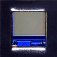
MT9V011P11STC:B Aptina LLC, MT9V011P11STC:B Datasheet - Page 21

MT9V011P11STC:B
Manufacturer Part Number
MT9V011P11STC:B
Description
SENSOR IMAGE VGA COLOR CMOS PLCC
Manufacturer
Aptina LLC
Series
DigitalClarity®, Micron®r
Type
CMOS Imagingr
Datasheets
1.MT9V011P11STCB.pdf
(33 pages)
2.MT9V011P11STCB.pdf
(2 pages)
3.MT9V011P11STCB.pdf
(2 pages)
Specifications of MT9V011P11STC:B
Pixel Size
5.6µm x 5.6µm
Active Pixel Array
640H x 480V
Frames Per Second
30
Voltage - Supply
2.8V
Package / Case
28-PLCC
Lead Free Status / RoHS Status
Lead free / RoHS Compliant
Other names
557-1315
Available stocks
Company
Part Number
Manufacturer
Quantity
Price
Company:
Part Number:
MT9V011P11STC:B
Manufacturer:
RENESAS
Quantity:
1 001
Part Number:
MT9V011P11STC:B
Manufacturer:
MICRON
Quantity:
20 000
Pixel Clock Speed
Reset
Digital Zoom
PDF: 817d5189/Source: 817d5173
MT9V011_C82S_2_PLCC.fm - Rev. B 1/05 EN
K = 2 when Reg0x07[4] = 1
In this expression the row time term corresponds to the number of rows integrated. The
overhead time is the time between the READ cycle and the RESET cycle, and the final
term is the effect of the reset delay.
Typically, the value of Reg0x09 (Shutter Width) is limited to the number of rows per
frame (which includes vertical blanking rows), such that the frame rate is not affected by
the integration time. If Reg0x09 is increased beyond the total number of rows per frame,
the MT9V011 will add additional blanking rows as needed. A second constraint is that
t
flicker, this means
t
Reg0x0A Pixel Clock Speed
The pixel clock speed is set by Reg0x0A. The pixel clock period will be the number set
plus two master clock cycles. The default value is 0, which is equal to 2 master clock
cycles. With a master clock frequency of 27 MHz the PIXCLK frequency will be 13.5 MHz.
The pixel clock out can be shifted relative to the data out by setting bit 8-11 of Reg0x07
appropriately.
Reg0x0D Reset
This register is used to reset the sensor to its default, power-up state. To reset the
MT9V011, first write a “1” into bit 0 of this register, then write a “0” into bit 0 to resume
operation.
Reg0x1E Digital Zoom/True decimation
In zoom mode, the pixel data rate is slowed down by a factor of either 2 or 4, and either 1
or 3 additional blank rows are added between each output row. This is designed to give
the controller logic time to repeat data to fill in a window that is either 2 or 4 times larger
with repeated data.
The pixel clock speed is not affected by this operation, and the output data for each pixel
is valid for either 2 or 4 pixel clocks. In zoom by 2 mode, every row is followed by a blank
row (with its own line valid, but all data bits = 0) of equal time. In zoom by 4 mode, every
row is followed by three blank rows. The combination of this register and an appropriate
change to the window sizing registers allows the user to zoom to a region of interest
without affecting the frame rate.
INT must be adjusted to avoid banding in the image from light flicker. Under 60 Hz
INT must be a multiple of 1/100 of a second.
t
INT must be a multiple of 1/120 of a second. Under 50 Hz flicker,
MT9V011 - 1/4-Inch VGA Digital Image Sensor
21
Micron Technology, Inc., reserves the right to change products or specifications without notice.
©2004 Micron Technology, Inc. All rights reserved.
Feature Description
Preliminary
‡


