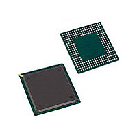
82P2288BB8 IDT, Integrated Device Technology Inc, 82P2288BB8 Datasheet - Page 17

82P2288BB8
Manufacturer Part Number
82P2288BB8
Description
Manufacturer
IDT, Integrated Device Technology Inc
Datasheet
1.82P2288BB8.pdf
(362 pages)
Specifications of 82P2288BB8
Screening Level
Industrial
Mounting
Surface Mount
Operating Temperature (min)
-40C
Operating Temperature (max)
85C
Lead Free Status / RoHS Status
Not Compliant
- Current page: 17 of 362
- Download datasheet (3Mb)
Note:
* This feature is available in ZB revision only.
Pin Description
IDT82P2288
TSCK[1] / MTSCK
CLK_GEN_1.544
CLK_GEN_2.048
CLK_SEL[0]
CLK_SEL[1]
CLK_SEL[2]
REFB_OUT
REFA_OUT
TSCK[2]
TSCK[3]
TSCK[4]
TSCK[5]
TSCK[6]
TSCK[7]
TSCK[8]
OSCO
Name
OSCI
Output / Input
Output
Output
Output
Output
Output
Type
Input
Input
Pin No.
C13
D15
C14
D14
B13
B15
A16
A15
B14
K3
K1
H2
H4
L3
L1
J3
J1
TSCK[1:8]: Transmit Side System Clock for Link 1 ~ 8
In Transmit Clock Master mode, TSCKn outputs a (gapped) 1.544 MHz (for T1/J1 mode) / 2.048 MHz (for E1 mode)
clock used to sample the signal on the corresponding TSDn and TSIGn pins and update the signal on the corre-
sponding TSFSn pin.
In Transmit Clock Slave mode, TSCKn inputs a 1.544 MHz (for T1/J1 mode only), 2.048 MHz or 4.096 MHz clock
used to sample the signal on the corresponding TSDn, TSIGn and TSFSn pins. Selected by the TSLVCK bit (b1, T1/
J1-010H / b1, E1-010H), the TSCK[1] can be used for all eight links.
MTSCK: Multiplexed Transmit Side System Clock for Link 1 ~ 8
In Transmit Multiplexed mode, MTSCK inputs a 8.192 MHz or 16.384 MHz clock used to sample the signal on the
corresponding MTSDA/MTSDB, MTSIGA/MTSIGB and MTSFS pins.
TSCK[1:8]/MTSCK are Schmitt-triggered inputs/outputs with pull-up resistors.
OSCI: Crystal Oscillator Input
This pin is connected to an external clock source. In T1 mode E1 Rate of Transmit System interface, this clock must
keep the source same with system transmit clock (TSCKn/MTSCK).
The clock frequency of OSCI is defined by CLK_SEL[2:0]. The clock accuracy should be ±32 ppm and duty cycle
should be from 40% to 60%.
OSCO: Crystal Oscillator Output
This pin outputs the inverted, buffered clock input from OSCI.
CLK_SEL[2:0]: Clock Selection
These three pins select the input clock signal:
When the CLK_SEL[2] pin is low, the input clock signal is N X 1.544 MHz;
When the CLK_SEL[2] pin is high, the input clock signal is N X 2.048 MHz.
When the CLK_SEL[1:0] pins are ‘00’, the N is 1;
When the CLK_SEL[1:0] pins are ‘01’, the N is 2;
When the CLK_SEL[1:0] pins are ‘10’, the N is 3;
When the CLK_SEL[1:0] pins are ‘11’, the N is 4.
CLK_SEL[2:0] are Schmitt-trigger inputs.
CLK_GEN_1.544: Clock Generator 1.544 MHz Output
This pin outputs the 1.544 MHz clock signal generated by the Clock Generator.
CLK_GEN_2.048: Clock Generator 2.048 MHz Output
This pin outputs the 2.048 MHz clock signal generated by the Clock Generator.
REFA_OUT: Reference Clock Output A
The frequecy is 2.048 MHz (E1) or 1.544 MHz (T1/J1)
When no LOS is detected, this pin outputs a recovered clock from the Clock and Data Recovery function block of
one of the eight links. The link is selected by the RO1[2:0] bits (b2~0, T1/J1-007H / b2~0, E1-007H).
When LOS is detected, this pin outputs MCLK or high level, as selected by the REFH_LOS bit (b0, T1/J1-03EH,... /
b0, E1-03EH,...). *
Note: MCLK is a clock derived from OSCI using an internal PLL, and the frequency is 2.048 MHz (E1) or 1.544 MHz
(T1/J1).
REFB_OUT: Reference Clock Output B
The frequecy is 2.048 MHz (E1) or 1.544 MHz (T1/J1)
When no LOS is detected, this pin outputs a recovered clock from the Clock and Data Recovery function block of
one of the eight links. The link is selected by the RO2[2:0] bits (b5~3, T1/J1-007H / b5~3, E1-007H).
When LOS is detected, this pin outputs MCLK or high level, as selected by the REFH_LOS bit (b0, T1/J1-03EH,... /
b0, E1-03EH,...). *
Clock Generator
17
OCTAL T1/E1/J1 LONG HAUL / SHORT HAUL TRANSCEIVER
Description
March 04, 2009
Related parts for 82P2288BB8
Image
Part Number
Description
Manufacturer
Datasheet
Request
R

Part Number:
Description:
TRANSLATION DEVICE DPI 80-PQFP
Manufacturer:
IDT, Integrated Device Technology Inc
Datasheet:

Part Number:
Description:
IDT PART
Manufacturer:
IDT, Integrated Device Technology Inc
Datasheet:

Part Number:
Description:
IC LIU T1/E1/J1 OCTAL 256PBGA
Manufacturer:
IDT, Integrated Device Technology Inc
Datasheet:

Part Number:
Description:
IC FREQ TIMING GENERATOR 28TSSOP
Manufacturer:
IDT, Integrated Device Technology Inc
Datasheet:

Part Number:
Description:
IC CLK DVR PLL 1:10 40VFQFPN
Manufacturer:
IDT, Integrated Device Technology Inc
Datasheet:

Part Number:
Description:
IC CLK FANOUT BUFFER 1:18 32LQFP
Manufacturer:
IDT, Integrated Device Technology Inc
Datasheet:

Part Number:
Description:
IC CLK FANOUT BUFFER 1:18 32LQFP
Manufacturer:
IDT, Integrated Device Technology Inc
Datasheet:

Part Number:
Description:
IC CK505 VREG/RES 56TSSOP
Manufacturer:
IDT, Integrated Device Technology Inc
Datasheet:

Part Number:
Description:
IC SDRAM CLK DVR 1:10 48-TSSOP
Manufacturer:
IDT, Integrated Device Technology Inc
Datasheet:

Part Number:
Description:
IC CLK DVR PLL 1:10 48TSSOP
Manufacturer:
IDT, Integrated Device Technology Inc
Datasheet:

Part Number:
Description:
IC FLEXPC CLK PROGR P4 56-TSSOP
Manufacturer:
IDT, Integrated Device Technology Inc
Datasheet:

Part Number:
Description:
IC FLEXPC CLK PROGR P4 56-TSSOP
Manufacturer:
IDT, Integrated Device Technology Inc
Datasheet:

Part Number:
Description:
IC FLEXPC CLK PROGR P4 56-SSOP
Manufacturer:
IDT, Integrated Device Technology Inc
Datasheet:

Part Number:
Description:
IC PLL CLK DRIVER 2.5V 28-TSSOP
Manufacturer:
IDT, Integrated Device Technology Inc
Datasheet:

Part Number:
Description:
IC CLOCK DRIVER 2.5V 24-TSSOP
Manufacturer:
IDT, Integrated Device Technology Inc
Datasheet:


