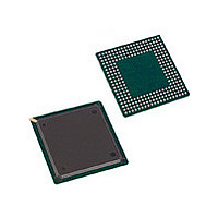
82P2288BB8 IDT, Integrated Device Technology Inc, 82P2288BB8 Datasheet - Page 266

82P2288BB8
Manufacturer Part Number
82P2288BB8
Description
Manufacturer
IDT, Integrated Device Technology Inc
Datasheet
1.82P2288BB8.pdf
(362 pages)
Specifications of 82P2288BB8
Screening Level
Industrial
Mounting
Surface Mount
Operating Temperature (min)
-40C
Operating Temperature (max)
85C
Lead Free Status / RoHS Status
Not Compliant
- Current page: 266 of 362
- Download datasheet (3Mb)
E1 RBIF Option Register (046H, 146H, 246H, 346H, 446H, 546H, 646H, 746H)
DE:
MRSDA(MRSDB) and MRSIGA(MRSIGB).
FE:
CMS:
bit of the eight links should be set to the same value.
TRI:
E1 RBIF Mode (047H, 147H, 247H, 347H, 447H, 547H, 647H, 747H)
RMODE:
Programming Information
IDT82P2288
Bit Name
Bit Name
This bit selects the active edge of RSCKn to update the data on RSDn and RSIGn and the active edge of MRSCK to update the data on
= 0: The falling edge is selected.
= 1: The rising edge is selected.
In Receive Multiplexed mode, the bit of the eight links should be set to the same value.
This bit selects the active edge of RSCKn to update/sample the pulse on RSFSn and the active edge of MRSCK to sample the pulse on MRSFS.
= 0: The falling edge is selected.
= 1: The rising edge is selected.
In Receive Multiplexed mode, the bit of the eight links should be set to the same value.
This bit is valid in Receive Clock Slave mode and Receive Multiplexed mode.
= 0: The speed of RSCKn/MRSCK is the same as the data rate on the system side (2.048 Mb/s / 8.192 Mb/s).
= 1: The speed of RSCKn/MRSCK is double the data rate on the system side (4.096 Mb/s / 16.384 Mb/s).
In Receive Clock Slave mode, if all eight links use the RSCK[1] and RSFS[1] to output the data (i.e., the RSLVCK bit (b, E1-01H) is set to ‘1’), the
In Receive Multiplexed mode, the bit of the eight links should be set to the same value.
= 0: The processed data and signaling bits are output on the RSDn/MRSDA(MRSDB) and RSIGn/MRSIGA(MRSIGB) pins respectively.
= 1: The output on the RSDn/MRSDA(MRSDB) and RSIGn/MRSIGA(MRSIGB) pins are in high impedance.
In Receive Non-multiplexed mode, this bit selects the sub-mode.
= 0: The Receive System Interface is operated in Receive Clock Master mode. The timing signal for clocking the data and the framing pulse to
align the data output on the RSDn pin are received from each line side.
= 1: The Receive System Interface is operated in Receive Clock Slave mode. The timing signal for clocking the data and the framing pulse to align
the data output on the RSDn pin are provided by the system side.
Default
Default
Bit No.
Bit No.
Type
Type
7
7
6
6
Reserved
5
5
Reserved
4
4
266
OCTAL T1/E1/J1 LONG HAUL / SHORT HAUL TRANSCEIVER
R/W
DE
3
1
3
R/W
FE
2
1
2
CMS
R/W
1
0
1
March 04, 2009
RMODE
R/W
R/W
TRI
0
1
0
1
Related parts for 82P2288BB8
Image
Part Number
Description
Manufacturer
Datasheet
Request
R

Part Number:
Description:
TRANSLATION DEVICE DPI 80-PQFP
Manufacturer:
IDT, Integrated Device Technology Inc
Datasheet:

Part Number:
Description:
IDT PART
Manufacturer:
IDT, Integrated Device Technology Inc
Datasheet:

Part Number:
Description:
IC LIU T1/E1/J1 OCTAL 256PBGA
Manufacturer:
IDT, Integrated Device Technology Inc
Datasheet:

Part Number:
Description:
IC FREQ TIMING GENERATOR 28TSSOP
Manufacturer:
IDT, Integrated Device Technology Inc
Datasheet:

Part Number:
Description:
IC CLK DVR PLL 1:10 40VFQFPN
Manufacturer:
IDT, Integrated Device Technology Inc
Datasheet:

Part Number:
Description:
IC CLK FANOUT BUFFER 1:18 32LQFP
Manufacturer:
IDT, Integrated Device Technology Inc
Datasheet:

Part Number:
Description:
IC CLK FANOUT BUFFER 1:18 32LQFP
Manufacturer:
IDT, Integrated Device Technology Inc
Datasheet:

Part Number:
Description:
IC CK505 VREG/RES 56TSSOP
Manufacturer:
IDT, Integrated Device Technology Inc
Datasheet:

Part Number:
Description:
IC SDRAM CLK DVR 1:10 48-TSSOP
Manufacturer:
IDT, Integrated Device Technology Inc
Datasheet:

Part Number:
Description:
IC CLK DVR PLL 1:10 48TSSOP
Manufacturer:
IDT, Integrated Device Technology Inc
Datasheet:

Part Number:
Description:
IC FLEXPC CLK PROGR P4 56-TSSOP
Manufacturer:
IDT, Integrated Device Technology Inc
Datasheet:

Part Number:
Description:
IC FLEXPC CLK PROGR P4 56-TSSOP
Manufacturer:
IDT, Integrated Device Technology Inc
Datasheet:

Part Number:
Description:
IC FLEXPC CLK PROGR P4 56-SSOP
Manufacturer:
IDT, Integrated Device Technology Inc
Datasheet:

Part Number:
Description:
IC PLL CLK DRIVER 2.5V 28-TSSOP
Manufacturer:
IDT, Integrated Device Technology Inc
Datasheet:

Part Number:
Description:
IC CLOCK DRIVER 2.5V 24-TSSOP
Manufacturer:
IDT, Integrated Device Technology Inc
Datasheet:


