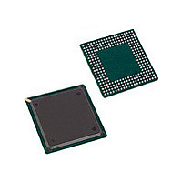
82P2288BB8 IDT, Integrated Device Technology Inc, 82P2288BB8 Datasheet - Page 98

82P2288BB8
Manufacturer Part Number
82P2288BB8
Description
Manufacturer
IDT, Integrated Device Technology Inc
Datasheet
1.82P2288BB8.pdf
(362 pages)
Specifications of 82P2288BB8
Screening Level
Industrial
Mounting
Surface Mount
Operating Temperature (min)
-40C
Operating Temperature (max)
85C
Lead Free Status / RoHS Status
Not Compliant
- Current page: 98 of 362
- Download datasheet (3Mb)
3.20.6 ALL ‘ZERO’S & ALL ‘ONE’S
the data stream if the TAIS bit and the TXDIS bit are set. The all zeros
transmission takes a higher priority.
3.20.7 CHANGE OF FRAME ALIGNMENT
lead to one-bit deletion or one-bit repetition in the data stream to be
transmitted, that is, to change the frame alignment position. The one-bit
deletion or repetition occurs randomly.
3.21 TRANSMIT BUFFER
timing is different from the line side timing in Transmit Slave mode.
source of the transmit clock can be selected in the recovered clock from
the line side, the processed clock from the backplane or the master
clock generated by the clock generator.
cally. The source of the transmit clock can be selected between the
recovered clock from the line side and the master clock generated by
the internal clock generator (1.544 MHz in T1/J1 mode or 2.048 MHz in
E1 mode). The selection is made by the XTS bit.
timing is 2.048 MHz from backplane and the line timing is 1.544 MHz
from the internal clock generator, the Transmit Buffer is selected auto-
matically to absorb high frequency mapping jitter due to the E1 to T1/J1
mapping scheme. In this case, 1.544 MHz must be locked to 2.048 MHz
by PLL of the internal clock generator. The XTS bit in the Transmit
Timing Option register does not take effect.
Functional Description
IDT82P2288
After all the above processes, all ’One’s or all ‘Zero’s will overwrite all
Any transition (from ‘0’ to ‘1’ or from ‘1’ to ‘0’) on the COFAEN bit will
Transmit Buffer can be used in the circumstances that backplane
The function of timing option is also integrated in this block. The
In Transmit Master mode, the Transmit Buffer is bypassed automati-
In Transmit Clock Slave T1/J1 mode E1 rate, for the backplane
98
OCTAL T1/E1/J1 LONG HAUL / SHORT HAUL TRANSCEIVER
bypassed and the source of the transmit clock selection are selected by
the XTS bit. When the XTS bit is set to ‘1’, line side timing is from
internal clock generator, but backplane timing is from backplane, so the
Transmit Buffer is selected to accommodate the different clocks. If these
two clocks are not locked, an internal slip will occur in the Transmit
Buffer. The source of the transmit clock is from the master clock gener-
ated by the internal clock generator (1.544 MHz in T1/J1 mode or 2.048
MHz in E1 mode). When the XTS bit is set to ‘0’, the line side timing is
also from the backplane timing, so the Transmit Buffer is bypassed. The
source of the transmit clock is from the processed clock from the back-
plane.
bypassed and the source of the transmit clock selection are the same as
that described in other Transmit Clock Slave modes.
be set to ‘0’ to bypass the Transmit Buffer (The Transmit Buffer is
selected automatically in T1/J1 mode E1 rate).
Table 57: Related Bit / Register In Chapter 3.20.6, Chapter 3.20.7 &
Chapter 3.21
In other Transmit Clock Slave modes, whether the Transmit Buffer is
In Transmit Multiplexed mode, whether the Transmit Buffer is
In most applications of Transmit Clock Slave mode, the XTS bit can
COFAEN
TXDIS
TAIS
XTS
Bit
Transmit Timing Option
FGEN Maintenance 1
Register
070, 170, 270, 370, 470,
06C, 16C, 26C, 36C,
46C, 56C, 66C, 76C
Address (Hex)
570, 670, 770
March 04, 2009
Related parts for 82P2288BB8
Image
Part Number
Description
Manufacturer
Datasheet
Request
R

Part Number:
Description:
TRANSLATION DEVICE DPI 80-PQFP
Manufacturer:
IDT, Integrated Device Technology Inc
Datasheet:

Part Number:
Description:
IDT PART
Manufacturer:
IDT, Integrated Device Technology Inc
Datasheet:

Part Number:
Description:
IC LIU T1/E1/J1 OCTAL 256PBGA
Manufacturer:
IDT, Integrated Device Technology Inc
Datasheet:

Part Number:
Description:
IC FREQ TIMING GENERATOR 28TSSOP
Manufacturer:
IDT, Integrated Device Technology Inc
Datasheet:

Part Number:
Description:
IC CLK DVR PLL 1:10 40VFQFPN
Manufacturer:
IDT, Integrated Device Technology Inc
Datasheet:

Part Number:
Description:
IC CLK FANOUT BUFFER 1:18 32LQFP
Manufacturer:
IDT, Integrated Device Technology Inc
Datasheet:

Part Number:
Description:
IC CLK FANOUT BUFFER 1:18 32LQFP
Manufacturer:
IDT, Integrated Device Technology Inc
Datasheet:

Part Number:
Description:
IC CK505 VREG/RES 56TSSOP
Manufacturer:
IDT, Integrated Device Technology Inc
Datasheet:

Part Number:
Description:
IC SDRAM CLK DVR 1:10 48-TSSOP
Manufacturer:
IDT, Integrated Device Technology Inc
Datasheet:

Part Number:
Description:
IC CLK DVR PLL 1:10 48TSSOP
Manufacturer:
IDT, Integrated Device Technology Inc
Datasheet:

Part Number:
Description:
IC FLEXPC CLK PROGR P4 56-TSSOP
Manufacturer:
IDT, Integrated Device Technology Inc
Datasheet:

Part Number:
Description:
IC FLEXPC CLK PROGR P4 56-TSSOP
Manufacturer:
IDT, Integrated Device Technology Inc
Datasheet:

Part Number:
Description:
IC FLEXPC CLK PROGR P4 56-SSOP
Manufacturer:
IDT, Integrated Device Technology Inc
Datasheet:

Part Number:
Description:
IC PLL CLK DRIVER 2.5V 28-TSSOP
Manufacturer:
IDT, Integrated Device Technology Inc
Datasheet:

Part Number:
Description:
IC CLOCK DRIVER 2.5V 24-TSSOP
Manufacturer:
IDT, Integrated Device Technology Inc
Datasheet:


