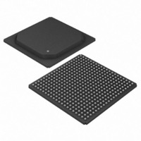
DS33R41+ Maxim Integrated Products, DS33R41+ Datasheet - Page 34

DS33R41+
Manufacturer Part Number
DS33R41+
Description
IC TXRX ETHERNET MAP 400-BGA
Manufacturer
Maxim Integrated Products
Type
Transceiverr
Datasheet
1.DS33R41.pdf
(335 pages)
Specifications of DS33R41+
Number Of Drivers/receivers
4/4
Protocol
T1/E1/J1
Voltage - Supply
3.14 V ~ 3.47 V
Mounting Type
Surface Mount
Package / Case
400-BGA
Lead Free Status / RoHS Status
Lead free / RoHS Compliant
- Current page: 34 of 335
- Download datasheet (2Mb)
DS33R41 Inverse-Multiplexing Ethernet Mapper with Quad Integrated T1/E1/J1 Transceivers
Both the transmit and receive path have two HDLC controllers. The HDLC controllers transmit and receive data via
the framer block. The HDLC controllers can be assigned to any time slot, group of time slots, portion of a time slot,
or to FDL (T1) or Sa bits (E1). Each controller has 128-bit FIFOs, thus reducing the amount of processor overhead
required to manage the flow of data. In addition, built-in support for reducing the processor time required handles
SS7 applications.
The backplane interface of the integrated transceivers provides a method of sending and receiving data from the
integrated Ethernet Mapper over an interleaved 8.192MHz TDM (IBO) bus. The Elastic Stores are required for IBO
operation, and manage slip conditions.
The parallel port provides access for control and configuration of all the transceiver’s features. Diagnostic
capabilities include loopbacks, PRBS pattern generation/detection, and 16-bit loop-up and loop-down code
generation and detection.
8.1 Processor Interface
Microprocessor control of the DS33R41 is accomplished through the interface pins of the microprocessor port. The
8-bit parallel data bus can be configured for Intel or Motorola modes of operation with the two MODEC[0:1] pins.
When MODEC = 00, bus timing is in Intel mode, as shown in
Figure 14-9
and
Figure
14-10. When MODEC = 01,
bus timing is in Motorola mode, as shown in
Figure 14-11
and
Figure
14-12. The address space is mapped
through the use of 10 address lines, A0 – A9. Multiplexed Mode is not supported on the processor interface.
The Chip Select (CS) pin must be brought to a logic low level to gain read and write access to the microprocessor
port of the Ethernet Mapper. The CST pin must be brought to a logic low level to gain read and write access to the
microprocessor port of the integrated T1/E1 transceivers. With Intel timing selected, the Read (RD) and Write (WR)
pins are used to indicate read and write operations and latch data through the interface. With Motorola timing
selected, the Read-Write (RW) pin is used to indicate read and write operations while the Data Strobe (DS) pin is
used to latch data through the interface.
The interrupt output pin (INT) is an open-drain output that will assert a logic-low level upon a number of software
maskable interrupt conditions. This pin is normally connected to the microprocessor interrupt input. The register
map is shown in
Table
12-1.
34 of 335
Related parts for DS33R41+
Image
Part Number
Description
Manufacturer
Datasheet
Request
R

Part Number:
Description:
MAX7528KCWPMaxim Integrated Products [CMOS Dual 8-Bit Buffered Multiplying DACs]
Manufacturer:
Maxim Integrated Products
Datasheet:

Part Number:
Description:
Single +5V, fully integrated, 1.25Gbps laser diode driver.
Manufacturer:
Maxim Integrated Products
Datasheet:

Part Number:
Description:
Single +5V, fully integrated, 155Mbps laser diode driver.
Manufacturer:
Maxim Integrated Products
Datasheet:

Part Number:
Description:
VRD11/VRD10, K8 Rev F 2/3/4-Phase PWM Controllers with Integrated Dual MOSFET Drivers
Manufacturer:
Maxim Integrated Products
Datasheet:

Part Number:
Description:
Highly Integrated Level 2 SMBus Battery Chargers
Manufacturer:
Maxim Integrated Products
Datasheet:

Part Number:
Description:
Current Monitor and Accumulator with Integrated Sense Resistor; ; Temperature Range: -40°C to +85°C
Manufacturer:
Maxim Integrated Products

Part Number:
Description:
TSSOP 14/A�/RS-485 Transceivers with Integrated 100O/120O Termination Resis
Manufacturer:
Maxim Integrated Products

Part Number:
Description:
TSSOP 14/A�/RS-485 Transceivers with Integrated 100O/120O Termination Resis
Manufacturer:
Maxim Integrated Products

Part Number:
Description:
QFN 16/A�/AC-DC and DC-DC Peak-Current-Mode Converters with Integrated Step
Manufacturer:
Maxim Integrated Products

Part Number:
Description:
TDFN/A/65V, 1A, 600KHZ, SYNCHRONOUS STEP-DOWN REGULATOR WITH INTEGRATED SWI
Manufacturer:
Maxim Integrated Products

Part Number:
Description:
Integrated Temperature Controller f
Manufacturer:
Maxim Integrated Products

Part Number:
Description:
SOT23-6/I�/45MHz to 650MHz, Integrated IF VCOs with Differential Output
Manufacturer:
Maxim Integrated Products

Part Number:
Description:
SOT23-6/I�/45MHz to 650MHz, Integrated IF VCOs with Differential Output
Manufacturer:
Maxim Integrated Products

Part Number:
Description:
EVALUATION KIT/2.4GHZ TO 2.5GHZ 802.11G/B RF TRANSCEIVER WITH INTEGRATED PA
Manufacturer:
Maxim Integrated Products

Part Number:
Description:
QFN/E/DUAL PCIE/SATA HIGH SPEED SWITCH WITH INTEGRATED BIAS RESISTOR
Manufacturer:
Maxim Integrated Products
Datasheet:


