C8051F540-TB Silicon Laboratories Inc, C8051F540-TB Datasheet - Page 198
C8051F540-TB
Manufacturer Part Number
C8051F540-TB
Description
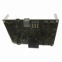
BOARD PROTOTYPE W/C8051F540
Manufacturer
Silicon Laboratories Inc
Type
MCUr
Specifications of C8051F540-TB
Contents
Board
Processor To Be Evaluated
C8051F54x
Processor Series
C8051F54x
Interface Type
USB
Operating Supply Voltage
5 V
Lead Free Status / RoHS Status
Lead free / RoHS Compliant
For Use With/related Products
C8051F54x
Lead Free Status / Rohs Status
Lead free / RoHS Compliant
Other names
336-1672


C8051F54x
20.5.1. Write Sequence (Master)
During a write sequence, an SMBus master writes data to a slave device. The master in this transfer will be
a transmitter during the address byte, and a transmitter during all data bytes. The SMBus interface gener-
ates the START condition and transmits the first byte containing the address of the target slave and the
data direction bit. In this case the data direction bit (R/W) will be logic 0 (WRITE). The master then trans-
mits one or more bytes of serial data. After each byte is transmitted, an acknowledge bit is generated by
the slave. The transfer is ended when the STO bit is set and a STOP is generated. Note that the interface
will switch to Master Receiver Mode if SMB0DAT is not written following a Master Transmitter interrupt.
Figure 20.5 shows a typical master write sequence. Two transmit data bytes are shown, though any num-
ber of bytes may be transmitted. Notice that all of the ‘data byte transferred’ interrupts occur after the ACK
cycle in this mode.
198
S
Received by SMBus
Interface
Transmitted by
SMBus Interface
SLA
Figure 20.5. Typical Master Write Sequence
W
A
Data Byte
Rev. 1.1
Interrupts
A
S = START
P = STOP
A = ACK
W = WRITE
SLA = Slave Address
Data Byte
A
P
Related parts for C8051F540-TB
Image
Part Number
Description
Manufacturer
Datasheet
Request
R

Part Number:
Description:
SMD/C°/SINGLE-ENDED OUTPUT SILICON OSCILLATOR
Manufacturer:
Silicon Laboratories Inc
Part Number:
Description:
Manufacturer:
Silicon Laboratories Inc
Datasheet:
Part Number:
Description:
N/A N/A/SI4010 AES KEYFOB DEMO WITH LCD RX
Manufacturer:
Silicon Laboratories Inc
Datasheet:
Part Number:
Description:
N/A N/A/SI4010 SIMPLIFIED KEY FOB DEMO WITH LED RX
Manufacturer:
Silicon Laboratories Inc
Datasheet:
Part Number:
Description:
N/A/-40 TO 85 OC/EZLINK MODULE; F930/4432 HIGH BAND (REV E/B1)
Manufacturer:
Silicon Laboratories Inc
Part Number:
Description:
EZLink Module; F930/4432 Low Band (rev e/B1)
Manufacturer:
Silicon Laboratories Inc
Part Number:
Description:
I°/4460 10 DBM RADIO TEST CARD 434 MHZ
Manufacturer:
Silicon Laboratories Inc
Part Number:
Description:
I°/4461 14 DBM RADIO TEST CARD 868 MHZ
Manufacturer:
Silicon Laboratories Inc
Part Number:
Description:
I°/4463 20 DBM RFSWITCH RADIO TEST CARD 460 MHZ
Manufacturer:
Silicon Laboratories Inc
Part Number:
Description:
I°/4463 20 DBM RADIO TEST CARD 868 MHZ
Manufacturer:
Silicon Laboratories Inc
Part Number:
Description:
I°/4463 27 DBM RADIO TEST CARD 868 MHZ
Manufacturer:
Silicon Laboratories Inc
Part Number:
Description:
I°/4463 SKYWORKS 30 DBM RADIO TEST CARD 915 MHZ
Manufacturer:
Silicon Laboratories Inc
Part Number:
Description:
N/A N/A/-40 TO 85 OC/4463 RFMD 30 DBM RADIO TEST CARD 915 MHZ
Manufacturer:
Silicon Laboratories Inc
Part Number:
Description:
I°/4463 20 DBM RADIO TEST CARD 169 MHZ
Manufacturer:
Silicon Laboratories Inc