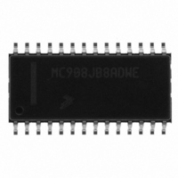
MC908JB8ADWE Freescale Semiconductor, MC908JB8ADWE Datasheet - Page 261

MC908JB8ADWE
Manufacturer Part Number
MC908JB8ADWE
Description
IC MCU 3MHZ 8K FLASH 28-SOIC
Manufacturer
Freescale Semiconductor
Series
HC08r
Datasheet
1.MC908JB8JDWE.pdf
(286 pages)
Specifications of MC908JB8ADWE
Core Processor
HC08
Core Size
8-Bit
Speed
3MHz
Connectivity
USB
Peripherals
LVD, POR, PWM
Number Of I /o
21
Program Memory Size
8KB (8K x 8)
Program Memory Type
FLASH
Ram Size
256 x 8
Voltage - Supply (vcc/vdd)
4 V ~ 5.5 V
Oscillator Type
Internal
Operating Temperature
0°C ~ 70°C
Package / Case
28-SOIC (7.5mm Width)
Processor Series
HC08JB
Core
HC08
Data Bus Width
8 bit
Data Ram Size
256 B
Interface Type
USB
Maximum Clock Frequency
3 MHz
Number Of Programmable I/os
37
Number Of Timers
2
Operating Supply Voltage
5.25 V
Maximum Operating Temperature
+ 70 C
Mounting Style
SMD/SMT
Development Tools By Supplier
FSICEBASE, DEMO908GZ60E, M68EML08GZE, KITUSBSPIDGLEVME, KITUSBSPIEVME, KIT33810EKEVME
Minimum Operating Temperature
0 C
Controller Family/series
HC08
No. Of I/o's
21
Ram Memory Size
256Byte
Cpu Speed
8MHz
No. Of Timers
1
Embedded Interface Type
SCI, SPI
Rohs Compliant
Yes
Lead Free Status / RoHS Status
Lead free / RoHS Compliant
Eeprom Size
-
Data Converters
-
Lead Free Status / Rohs Status
Lead free / RoHS Compliant
Available stocks
Company
Part Number
Manufacturer
Quantity
Price
Part Number:
MC908JB8ADWE
Manufacturer:
FREESCALE
Quantity:
20 000
- Current page: 261 of 286
- Download datasheet (2Mb)
18.13 Memory Characteristics
MC68HC908JB8•MC68HC08JB8•MC68HC08JT8 — Rev. 2.3
Freescale Semiconductor
NOTES:
RAM data retention voltage
FLASH block size
FLASH programming size
FLASH read bus clock frequency
FLASH block erase time
FLASH mass erase time
FLASH PGM/ERASE to HVEN set up time
FLASH high-voltage hold time
FLASH high-voltage hold time (mass erase)
FLASH program hold time
FLASH program time
FLASH return to read time
FLASH cumulative program hv period
FLASH row erase endurance
FLASH row program endurance
FLASH data retention time
1. f
2. If the page erase time is longer than t
3. If the mass erase time is longer than t
4. t
5. t
6. The minimum row endurance value specifies each row of the FLASH memory is guaranteed to work for at least this many
7. The minimum row endurance value specifies each row of the FLASH memory is guaranteed to work for at least this many
8. The FLASH is guaranteed to retain data over the entire operating temperature range for at least the minimum time speci-
ory
erase / program cycles.
erase / program cycles.
fied.
READ
rcv
HV
is defined as the time it need before start the read of the flash after turn off the HVEN bit
is defined as the cumulative high voltage programming time to the same row before next erase
is defined as the frequency range for which the FLASH memory can be read.
Characteristic
(8)
(6)
(7)
Erase
MErase
(Min), there is no erase-disturb, but it reduced the endurance of the flash memory
(Min), there is no erase-disturb, but it reduced the endurance of the flash mem-
Electrical Specifications
t
Symbol
MErase
t
f
Erase
Read
t
V
t
t
PROG
t
rcv
HV
t
t
t
nvhl
RDR
—
nvs
nvh
pgs
—
—
—
—
(4)
(5)
(1)
(2)
(3)
32 k
Min
100
10k
10k
1.3
10
20
10
—
2
2
5
5
1
512
64
Electrical Specifications
Memory Characteristics
8.4 M
Max
25
—
—
—
—
—
—
—
—
—
—
—
—
Technical Data
Cycles
Cycles
Bytes
Bytes
Years
Unit
ms
ms
ms
Hz
µs
µs
µs
µs
µs
µs
V
261
Related parts for MC908JB8ADWE
Image
Part Number
Description
Manufacturer
Datasheet
Request
R
Part Number:
Description:
Manufacturer:
Freescale Semiconductor, Inc
Datasheet:
Part Number:
Description:
Manufacturer:
Freescale Semiconductor, Inc
Datasheet:
Part Number:
Description:
Manufacturer:
Freescale Semiconductor, Inc
Datasheet:
Part Number:
Description:
Manufacturer:
Freescale Semiconductor, Inc
Datasheet:
Part Number:
Description:
Manufacturer:
Freescale Semiconductor, Inc
Datasheet:
Part Number:
Description:
Manufacturer:
Freescale Semiconductor, Inc
Datasheet:
Part Number:
Description:
Manufacturer:
Freescale Semiconductor, Inc
Datasheet:
Part Number:
Description:
Manufacturer:
Freescale Semiconductor, Inc
Datasheet:
Part Number:
Description:
Manufacturer:
Freescale Semiconductor, Inc
Datasheet:
Part Number:
Description:
Manufacturer:
Freescale Semiconductor, Inc
Datasheet:
Part Number:
Description:
Manufacturer:
Freescale Semiconductor, Inc
Datasheet:
Part Number:
Description:
Manufacturer:
Freescale Semiconductor, Inc
Datasheet:
Part Number:
Description:
Manufacturer:
Freescale Semiconductor, Inc
Datasheet:
Part Number:
Description:
Manufacturer:
Freescale Semiconductor, Inc
Datasheet:
Part Number:
Description:
Manufacturer:
Freescale Semiconductor, Inc
Datasheet:


