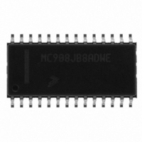
MC908JB8ADWE Freescale Semiconductor, MC908JB8ADWE Datasheet - Page 275

MC908JB8ADWE
Manufacturer Part Number
MC908JB8ADWE
Description
IC MCU 3MHZ 8K FLASH 28-SOIC
Manufacturer
Freescale Semiconductor
Series
HC08r
Datasheet
1.MC908JB8JDWE.pdf
(286 pages)
Specifications of MC908JB8ADWE
Core Processor
HC08
Core Size
8-Bit
Speed
3MHz
Connectivity
USB
Peripherals
LVD, POR, PWM
Number Of I /o
21
Program Memory Size
8KB (8K x 8)
Program Memory Type
FLASH
Ram Size
256 x 8
Voltage - Supply (vcc/vdd)
4 V ~ 5.5 V
Oscillator Type
Internal
Operating Temperature
0°C ~ 70°C
Package / Case
28-SOIC (7.5mm Width)
Processor Series
HC08JB
Core
HC08
Data Bus Width
8 bit
Data Ram Size
256 B
Interface Type
USB
Maximum Clock Frequency
3 MHz
Number Of Programmable I/os
37
Number Of Timers
2
Operating Supply Voltage
5.25 V
Maximum Operating Temperature
+ 70 C
Mounting Style
SMD/SMT
Development Tools By Supplier
FSICEBASE, DEMO908GZ60E, M68EML08GZE, KITUSBSPIDGLEVME, KITUSBSPIEVME, KIT33810EKEVME
Minimum Operating Temperature
0 C
Controller Family/series
HC08
No. Of I/o's
21
Ram Memory Size
256Byte
Cpu Speed
8MHz
No. Of Timers
1
Embedded Interface Type
SCI, SPI
Rohs Compliant
Yes
Lead Free Status / RoHS Status
Lead free / RoHS Compliant
Eeprom Size
-
Data Converters
-
Lead Free Status / Rohs Status
Lead free / RoHS Compliant
Available stocks
Company
Part Number
Manufacturer
Quantity
Price
Part Number:
MC908JB8ADWE
Manufacturer:
FREESCALE
Quantity:
20 000
- Current page: 275 of 286
- Download datasheet (2Mb)
A.7.2 Memory Characteristics
A.8 MC68HC08JB8 Order Numbers
MC68HC908JB8•MC68HC08JB8•MC68HC08JT8 — Rev. 2.3
Freescale Semiconductor
NOTES:
RAM data retention voltage
Notes:
1. V
2. Typical values reflect average measurements at midpoint of voltage range, 25 °C only.
3. Run (operating) I
4. Wait I
5. STOP I
6. Maximum is highest voltage that POR is guaranteed.
7. If minimum V
Since MC68HC08JB8 is a ROM device, FLASH memory electrical characteristics do not apply.
loads. Less than 100 pF on all outputs. C
affects run I
than 100 pF on all outputs. C
as inputs; OSC2 capacitance linearly affects wait I
and D– pins and 15 kΩ ± 5% termination resistor on D+ pin; no port pins sourcing current.
V
DD
REG
= 4.0 to 5.5 Vdc, V
DD
is reached.
DD
measured using external square wave clock source (f
measured with USB in suspend mode; OSC1 grounded; transceiver pullup resistor of 1.5 kΩ ± 5% between V
DD
REG
. Measured with all modules enabled.
DD
is not reached before the internal POR reset is released, RST must be driven low externally until minimum
measured using external square wave clock source (f
Characteristic
SS
= 0 Vdc, T
These part numbers are generic numbers only. To place an order, ROM
code must be submitted to the ROM Processing Center (RPC).
L
MC68HC08JB8JP
MC68HC08JB8JDW
MC68HC08JB8ADW
MC68HC08JB8FB
= 20 pF on OSC2; 15 kΩ ± 5% termination resistors on D+ and D– pins; all ports configured
MC Order Number
A
= T
L
L
to T
= 20 pF on OSC2. All ports configured as inputs. OSC2 capacitance linearly
Table A-2. MC68HC08JB8 Order Numbers
H
, unless otherwise noted.
DD
MC68HC08JB8
XCLK
Symbol
= 6 MHz); all inputs 0.2 V from rail; no dc loads; less
20-pin SOIC
28-pin SOIC
20-pin PDIP
44-pin QFP
V
Package
RDR
XCLK
= 6 MHz). All inputs 0.2 V from rail. No dc
Min
1.3
Temperature Range
0 to +70 °C
0 to +70 °C
0 to +70 °C
0 to +70 °C
Max
Operating
—
MC68HC08JB8
Technical Data
Unit
V
REG
275
Related parts for MC908JB8ADWE
Image
Part Number
Description
Manufacturer
Datasheet
Request
R
Part Number:
Description:
Manufacturer:
Freescale Semiconductor, Inc
Datasheet:
Part Number:
Description:
Manufacturer:
Freescale Semiconductor, Inc
Datasheet:
Part Number:
Description:
Manufacturer:
Freescale Semiconductor, Inc
Datasheet:
Part Number:
Description:
Manufacturer:
Freescale Semiconductor, Inc
Datasheet:
Part Number:
Description:
Manufacturer:
Freescale Semiconductor, Inc
Datasheet:
Part Number:
Description:
Manufacturer:
Freescale Semiconductor, Inc
Datasheet:
Part Number:
Description:
Manufacturer:
Freescale Semiconductor, Inc
Datasheet:
Part Number:
Description:
Manufacturer:
Freescale Semiconductor, Inc
Datasheet:
Part Number:
Description:
Manufacturer:
Freescale Semiconductor, Inc
Datasheet:
Part Number:
Description:
Manufacturer:
Freescale Semiconductor, Inc
Datasheet:
Part Number:
Description:
Manufacturer:
Freescale Semiconductor, Inc
Datasheet:
Part Number:
Description:
Manufacturer:
Freescale Semiconductor, Inc
Datasheet:
Part Number:
Description:
Manufacturer:
Freescale Semiconductor, Inc
Datasheet:
Part Number:
Description:
Manufacturer:
Freescale Semiconductor, Inc
Datasheet:
Part Number:
Description:
Manufacturer:
Freescale Semiconductor, Inc
Datasheet:


