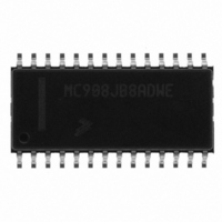
MC908JB8ADWE Freescale Semiconductor, MC908JB8ADWE Datasheet - Page 284

MC908JB8ADWE
Manufacturer Part Number
MC908JB8ADWE
Description
IC MCU 3MHZ 8K FLASH 28-SOIC
Manufacturer
Freescale Semiconductor
Series
HC08r
Datasheet
1.MC908JB8JDWE.pdf
(286 pages)
Specifications of MC908JB8ADWE
Core Processor
HC08
Core Size
8-Bit
Speed
3MHz
Connectivity
USB
Peripherals
LVD, POR, PWM
Number Of I /o
21
Program Memory Size
8KB (8K x 8)
Program Memory Type
FLASH
Ram Size
256 x 8
Voltage - Supply (vcc/vdd)
4 V ~ 5.5 V
Oscillator Type
Internal
Operating Temperature
0°C ~ 70°C
Package / Case
28-SOIC (7.5mm Width)
Processor Series
HC08JB
Core
HC08
Data Bus Width
8 bit
Data Ram Size
256 B
Interface Type
USB
Maximum Clock Frequency
3 MHz
Number Of Programmable I/os
37
Number Of Timers
2
Operating Supply Voltage
5.25 V
Maximum Operating Temperature
+ 70 C
Mounting Style
SMD/SMT
Development Tools By Supplier
FSICEBASE, DEMO908GZ60E, M68EML08GZE, KITUSBSPIDGLEVME, KITUSBSPIEVME, KIT33810EKEVME
Minimum Operating Temperature
0 C
Controller Family/series
HC08
No. Of I/o's
21
Ram Memory Size
256Byte
Cpu Speed
8MHz
No. Of Timers
1
Embedded Interface Type
SCI, SPI
Rohs Compliant
Yes
Lead Free Status / RoHS Status
Lead free / RoHS Compliant
Eeprom Size
-
Data Converters
-
Lead Free Status / Rohs Status
Lead free / RoHS Compliant
Available stocks
Company
Part Number
Manufacturer
Quantity
Price
Part Number:
MC908JB8ADWE
Manufacturer:
FREESCALE
Quantity:
20 000
- Current page: 284 of 286
- Download datasheet (2Mb)
MC68HC08JT8
B.11.4 Control Timing
B.11.5 Memory Characteristics
B.12 MC68HC08JT8 Order Numbers
Technical Data
284
NOTES:
Internal operating frequency
RAM data retention voltage
NOTES: Since MC68HC08JT8 is a ROM device, FLASH memory electrical characteristics do not apply.
2. Typical values reflect average measurements at 3V, 25 °C only.
3. In LDD mode, the specified I
5. Wait I
6. Stop I
1. V
4. Run (operating) I
7. Maximum is highest voltage that POR is guaranteed.
V
loads. Less than 100 pF on all outputs. C
affects run I
than 100 pF on all outputs. C
V
V
DD
OL
DD
DD
= 2.0 to 3.6 Vdc, V
+ voltage dropped across LED.
= 2.0V
= 3.0V
DD
DD
measured using external square wave clock source (f
measured with OSC1 grounded; no port pins sourcing current.
MC68HC08JT8ADW
MC68HC08JT8FB
MC68HC08JT8FBE
DD
MC Order Number
. Measured with all modules enabled.
DD
measured using external square wave clock source (f
Characteristic
Characteristic
SS
= 0 Vdc, T
These part numbers are generic numbers only. To place an order, ROM
code must be submitted to the ROM Processing Center (RPC).
OL
L
= 20 pF on OSC2. All ports configured as inputs. OSC2 capacitance linearly affects wait I
is achieved when the external pullup voltage is equal to or higher than the voltage:
Table B-2. MC68HC08JT8 Order Numbers
A
= T
L
L
to T
= 20 pF on OSC2. All ports configured as inputs. OSC2 capacitance linearly
28-pin SOIC
44-pin QFP
44-pin QFP
Package
H
, unless otherwise noted.
MC68HC08JT8
MC68HC908JB8•MC68HC08JB8•MC68HC08JT8 — Rev. 2.3
XCLK
Temperature Range
Symbol
Symbol
= 6 MHz). All inputs 0.2 V from rail. No dc loads. Less
V
f
RDR
OP
0 to +70 °C
0 to +70 °C
0 to +70 °C
Operating
XCLK
= 6 MHz). All inputs 0.2 V from rail. No dc
Min
Min
1.3
—
—
Freescale Semiconductor
Pb-Free and RoHS
Max
Max
2.5
3.0
—
Compliance
compliant.
—
MHz
MHz
Unit
Unit
V
DD
.
Related parts for MC908JB8ADWE
Image
Part Number
Description
Manufacturer
Datasheet
Request
R
Part Number:
Description:
Manufacturer:
Freescale Semiconductor, Inc
Datasheet:
Part Number:
Description:
Manufacturer:
Freescale Semiconductor, Inc
Datasheet:
Part Number:
Description:
Manufacturer:
Freescale Semiconductor, Inc
Datasheet:
Part Number:
Description:
Manufacturer:
Freescale Semiconductor, Inc
Datasheet:
Part Number:
Description:
Manufacturer:
Freescale Semiconductor, Inc
Datasheet:
Part Number:
Description:
Manufacturer:
Freescale Semiconductor, Inc
Datasheet:
Part Number:
Description:
Manufacturer:
Freescale Semiconductor, Inc
Datasheet:
Part Number:
Description:
Manufacturer:
Freescale Semiconductor, Inc
Datasheet:
Part Number:
Description:
Manufacturer:
Freescale Semiconductor, Inc
Datasheet:
Part Number:
Description:
Manufacturer:
Freescale Semiconductor, Inc
Datasheet:
Part Number:
Description:
Manufacturer:
Freescale Semiconductor, Inc
Datasheet:
Part Number:
Description:
Manufacturer:
Freescale Semiconductor, Inc
Datasheet:
Part Number:
Description:
Manufacturer:
Freescale Semiconductor, Inc
Datasheet:
Part Number:
Description:
Manufacturer:
Freescale Semiconductor, Inc
Datasheet:
Part Number:
Description:
Manufacturer:
Freescale Semiconductor, Inc
Datasheet:


