MC908JB8ADWE Freescale Semiconductor, MC908JB8ADWE Datasheet - Page 54
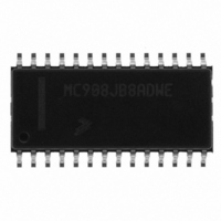
MC908JB8ADWE
Manufacturer Part Number
MC908JB8ADWE
Description
IC MCU 3MHZ 8K FLASH 28-SOIC
Manufacturer
Freescale Semiconductor
Series
HC08r
Datasheet
1.MC908JB8JDWE.pdf
(286 pages)
Specifications of MC908JB8ADWE
Core Processor
HC08
Core Size
8-Bit
Speed
3MHz
Connectivity
USB
Peripherals
LVD, POR, PWM
Number Of I /o
21
Program Memory Size
8KB (8K x 8)
Program Memory Type
FLASH
Ram Size
256 x 8
Voltage - Supply (vcc/vdd)
4 V ~ 5.5 V
Oscillator Type
Internal
Operating Temperature
0°C ~ 70°C
Package / Case
28-SOIC (7.5mm Width)
Processor Series
HC08JB
Core
HC08
Data Bus Width
8 bit
Data Ram Size
256 B
Interface Type
USB
Maximum Clock Frequency
3 MHz
Number Of Programmable I/os
37
Number Of Timers
2
Operating Supply Voltage
5.25 V
Maximum Operating Temperature
+ 70 C
Mounting Style
SMD/SMT
Development Tools By Supplier
FSICEBASE, DEMO908GZ60E, M68EML08GZE, KITUSBSPIDGLEVME, KITUSBSPIEVME, KIT33810EKEVME
Minimum Operating Temperature
0 C
Controller Family/series
HC08
No. Of I/o's
21
Ram Memory Size
256Byte
Cpu Speed
8MHz
No. Of Timers
1
Embedded Interface Type
SCI, SPI
Rohs Compliant
Yes
Lead Free Status / RoHS Status
Lead free / RoHS Compliant
Eeprom Size
-
Data Converters
-
Lead Free Status / Rohs Status
Lead free / RoHS Compliant
Available stocks
Company
Part Number
Manufacturer
Quantity
Price

Part Number:
MC908JB8ADWE
Manufacturer:
FREESCALE
Quantity:
20 000


FLASH Memory
4.3 Functional Description
Technical Data
54
Addr.
$FE08
$FE09
FLASH Control Register
Register Name
FLASH Block Protect
NOTE:
(FLBPR)
Register
(FLCR)
Figure 4-1. FLASH Memory Register Summary
The FLASH memory consists of an array of 8,192 bytes for user memory
plus a small block of 16 bytes for user interrupt vectors.
reads as logic 1 and a programmed bit reads as a logic 0.
memory is block erasable. The minimum erase block size is 512 bytes.
Program and erase operation operations are facilitated through control
bits in FLASH control register (FLCR).The address ranges for the
FLASH memory are shown as follows:
Programming tools are available from Freescale. Contact your local
Freescale representative for more information.
A security feature prevents viewing of the FLASH contents.
1. No security feature is absolutely secure. However, Freescale’s strategy is to make reading or
copying the FLASH difficult for unauthorized users.
Reset:
Reset:
Read:
Read:
Write:
Write:
•
•
$DC00–$FBFF (user memory; 8,192 bytes)
$FFF0–$FFFF (user interrupt vectors; 16 bytes)
Bit 7
BPR7
0
0
0
BPR6
FLASH Memory
6
0
0
0
MC68HC908JB8•MC68HC08JB8•MC68HC08JT8 — Rev. 2.3
BPR5
5
0
0
0
BPR4
4
0
0
0
HVEN
BPR3
3
0
0
MASS
BPR2
Freescale Semiconductor
2
0
0
An erased bit
ERASE
BPR1
The FLASH
1
0
0
1
Bit 0
BPR0
PGM
0
0
Related parts for MC908JB8ADWE
Image
Part Number
Description
Manufacturer
Datasheet
Request
R

Part Number:
Description:
Manufacturer:
Freescale Semiconductor, Inc
Datasheet:
Part Number:
Description:
Manufacturer:
Freescale Semiconductor, Inc
Datasheet:
Part Number:
Description:
Manufacturer:
Freescale Semiconductor, Inc
Datasheet:
Part Number:
Description:
Manufacturer:
Freescale Semiconductor, Inc
Datasheet:
Part Number:
Description:
Manufacturer:
Freescale Semiconductor, Inc
Datasheet:
Part Number:
Description:
Manufacturer:
Freescale Semiconductor, Inc
Datasheet:
Part Number:
Description:
Manufacturer:
Freescale Semiconductor, Inc
Datasheet:
Part Number:
Description:
Manufacturer:
Freescale Semiconductor, Inc
Datasheet:
Part Number:
Description:
Manufacturer:
Freescale Semiconductor, Inc
Datasheet:
Part Number:
Description:
Manufacturer:
Freescale Semiconductor, Inc
Datasheet:
Part Number:
Description:
Manufacturer:
Freescale Semiconductor, Inc
Datasheet:
Part Number:
Description:
Manufacturer:
Freescale Semiconductor, Inc
Datasheet:
Part Number:
Description:
Manufacturer:
Freescale Semiconductor, Inc
Datasheet:
Part Number:
Description:
Manufacturer:
Freescale Semiconductor, Inc
Datasheet:
Part Number:
Description:
Manufacturer:
Freescale Semiconductor, Inc
Datasheet: