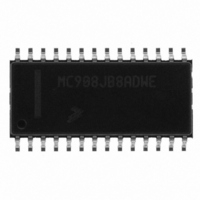
MC908JB8ADWE Freescale Semiconductor, MC908JB8ADWE Datasheet - Page 91

MC908JB8ADWE
Manufacturer Part Number
MC908JB8ADWE
Description
IC MCU 3MHZ 8K FLASH 28-SOIC
Manufacturer
Freescale Semiconductor
Series
HC08r
Datasheet
1.MC908JB8JDWE.pdf
(286 pages)
Specifications of MC908JB8ADWE
Core Processor
HC08
Core Size
8-Bit
Speed
3MHz
Connectivity
USB
Peripherals
LVD, POR, PWM
Number Of I /o
21
Program Memory Size
8KB (8K x 8)
Program Memory Type
FLASH
Ram Size
256 x 8
Voltage - Supply (vcc/vdd)
4 V ~ 5.5 V
Oscillator Type
Internal
Operating Temperature
0°C ~ 70°C
Package / Case
28-SOIC (7.5mm Width)
Processor Series
HC08JB
Core
HC08
Data Bus Width
8 bit
Data Ram Size
256 B
Interface Type
USB
Maximum Clock Frequency
3 MHz
Number Of Programmable I/os
37
Number Of Timers
2
Operating Supply Voltage
5.25 V
Maximum Operating Temperature
+ 70 C
Mounting Style
SMD/SMT
Development Tools By Supplier
FSICEBASE, DEMO908GZ60E, M68EML08GZE, KITUSBSPIDGLEVME, KITUSBSPIEVME, KIT33810EKEVME
Minimum Operating Temperature
0 C
Controller Family/series
HC08
No. Of I/o's
21
Ram Memory Size
256Byte
Cpu Speed
8MHz
No. Of Timers
1
Embedded Interface Type
SCI, SPI
Rohs Compliant
Yes
Lead Free Status / RoHS Status
Lead free / RoHS Compliant
Eeprom Size
-
Data Converters
-
Lead Free Status / Rohs Status
Lead free / RoHS Compliant
Available stocks
Company
Part Number
Manufacturer
Quantity
Price
Part Number:
MC908JB8ADWE
Manufacturer:
FREESCALE
Quantity:
20 000
- Current page: 91 of 286
- Download datasheet (2Mb)
7.4 I/O Signals
7.4.1 Crystal Amplifier Input Pin (OSC1)
7.4.2 Crystal Amplifier Output Pin (OSC2)
7.4.3 Oscillator Enable Signal (SIMOSCEN)
7.4.4 External Clock Source (OSCXCLK)
MC68HC908JB8•MC68HC08JB8•MC68HC08JT8 — Rev. 2.3
Freescale Semiconductor
The series resistor (R
oscillator guidelines and may not be required for all ranges of operation,
especially with high-frequency crystals. Refer to the crystal
manufacturer’s data for more information.
The following paragraphs describe the oscillator input/output (I/O)
signals.
The OSC1 pin is an input to the crystal oscillator amplifier.
The OSC2 pin is the output of the crystal oscillator inverting amplifier.
The SIMOSCEN signal comes from the system integration module (SIM)
and enables the oscillator.
The crystal oscillator output signal passes through the clock doubler and
OSCXCLK is the output signal of the clock doubler. OSCXCLK runs at
twice the speed of the crystal (f
relation of OSCXCLK to OSC1 and OSC2 and may not represent the
actual circuitry. The duty cycle of OSCXCLK is unknown and may
depend on the crystal and other external factors. Also, the frequency and
amplitude of OSCXCLK can be unstable at startup.
Oscillator (OSC)
S
) is included in the diagram to follow strict Pierce
XCLK
).
Figure 7-1
shows only the logical
Oscillator (OSC)
Technical Data
I/O Signals
91
Related parts for MC908JB8ADWE
Image
Part Number
Description
Manufacturer
Datasheet
Request
R
Part Number:
Description:
Manufacturer:
Freescale Semiconductor, Inc
Datasheet:
Part Number:
Description:
Manufacturer:
Freescale Semiconductor, Inc
Datasheet:
Part Number:
Description:
Manufacturer:
Freescale Semiconductor, Inc
Datasheet:
Part Number:
Description:
Manufacturer:
Freescale Semiconductor, Inc
Datasheet:
Part Number:
Description:
Manufacturer:
Freescale Semiconductor, Inc
Datasheet:
Part Number:
Description:
Manufacturer:
Freescale Semiconductor, Inc
Datasheet:
Part Number:
Description:
Manufacturer:
Freescale Semiconductor, Inc
Datasheet:
Part Number:
Description:
Manufacturer:
Freescale Semiconductor, Inc
Datasheet:
Part Number:
Description:
Manufacturer:
Freescale Semiconductor, Inc
Datasheet:
Part Number:
Description:
Manufacturer:
Freescale Semiconductor, Inc
Datasheet:
Part Number:
Description:
Manufacturer:
Freescale Semiconductor, Inc
Datasheet:
Part Number:
Description:
Manufacturer:
Freescale Semiconductor, Inc
Datasheet:
Part Number:
Description:
Manufacturer:
Freescale Semiconductor, Inc
Datasheet:
Part Number:
Description:
Manufacturer:
Freescale Semiconductor, Inc
Datasheet:
Part Number:
Description:
Manufacturer:
Freescale Semiconductor, Inc
Datasheet:


