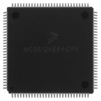
MC9S12NE64CPV Freescale Semiconductor, MC9S12NE64CPV Datasheet - Page 263

MC9S12NE64CPV
Manufacturer Part Number
MC9S12NE64CPV
Description
IC MCU 25MHZ ETHERNT/PHY 112LQFP
Manufacturer
Freescale Semiconductor
Series
HCS12r
Datasheet
1.MC9S12NE64VTU.pdf
(554 pages)
Specifications of MC9S12NE64CPV
Mfg Application Notes
MC9S12NE64 Integrated Ethernet Controller Implementing an Ethernet Interface with the MC9S12NE64 Web Server Development with MC9S12NE64 and Open TCP
Core Processor
HCS12
Core Size
16-Bit
Speed
25MHz
Connectivity
EBI/EMI, Ethernet, I²C, SCI, SPI
Peripherals
POR, PWM, WDT
Number Of I /o
70
Program Memory Size
64KB (64K x 8)
Program Memory Type
FLASH
Ram Size
8K x 8
Voltage - Supply (vcc/vdd)
2.375 V ~ 3.465 V
Data Converters
A/D 8x10b
Oscillator Type
Internal
Operating Temperature
-40°C ~ 85°C
Package / Case
112-LQFP
Data Bus Width
16 bit
Data Ram Size
8 KB
Interface Type
I2C, SCI, SPI
Maximum Clock Frequency
25 MHz
Number Of Programmable I/os
70
Number Of Timers
16 bit
Operating Supply Voltage
- 0.3 V to + 3 V
Maximum Operating Temperature
+ 105 C
Mounting Style
SMD/SMT
Minimum Operating Temperature
- 65 C
On-chip Adc
10 bit
For Use With
EVB9S12NE64E - BOARD EVAL FOR 9S12NE64DEMO9S12NE64E - DEMO BOARD FOR 9S12NE64
Lead Free Status / RoHS Status
Contains lead / RoHS non-compliant
Eeprom Size
-
Lead Free Status / Rohs Status
No RoHS Version Available
Available stocks
Company
Part Number
Manufacturer
Quantity
Price
Company:
Part Number:
MC9S12NE64CPV
Manufacturer:
RENESAS
Quantity:
21 000
Company:
Part Number:
MC9S12NE64CPV
Manufacturer:
FREESCAL
Quantity:
455
Company:
Part Number:
MC9S12NE64CPV
Manufacturer:
Freescale Semiconductor
Quantity:
10 000
Company:
Part Number:
MC9S12NE64CPVE
Manufacturer:
ST
Quantity:
445
Company:
Part Number:
MC9S12NE64CPVE
Manufacturer:
Freescale Semiconductor
Quantity:
10 000
- Current page: 263 of 554
- Download datasheet (4Mb)
9.2.2
This pin is used to transmit data out of the SPI module when it is configured as a slave and receive data
when it is configured as master.
9.2.3
This pin is used to output the select signal from the SPI module to another peripheral with which a data
transfer is to take place when its configured as a master and its used as an input to receive the slave select
signal when the SPI is configured as slave.
9.2.4
This pin is used to output the clock with respect to which the SPI transfers data or receive clock in case of
slave.
9.3
This section provides a detailed description of address space and registers used by the SPI.
The memory map for the SPIV3 is given below in
of a base address and an address offset. The base address is defined at the SoC level and the address offset
is defined at the module level. Reads from the reserved bits return zeros and writes to the reserved bits have
no effect.
9.3.1
Freescale Semiconductor
1
2
3
Certain bits are non-writable.
Writes to this register are ignored.
Reading from this register returns all zeros.
Memory Map and Register Definition
Address
0x0000
0x0001
0x0002
0x0003
0x0004
0x0005
0x0006
0x0007
MISO — Master In/Slave Out Pin
SCK — Serial Clock Pin
Module Memory Map
SS — Slave Select Pin
SPI Control Register 1 (SPICR1)
SPI Control Register 2 (SPICR2)
SPI Baud Rate Register (SPIBR)
SPI Status Register (SPISR)
Reserved
SPI Data Register (SPIDR)
Reserved
Reserved
MC9S12NE64 Data Sheet, Rev. 1.1
Table 9-1. SPIV3 Memory Map
Table
Use
9-1. The address listed for each register is the sum
Memory Map and Register Definition
Access
R/W
R/W
—
—
—
R/W
R/W
R
2,3
2,3
2,3
2
1
1
263
Related parts for MC9S12NE64CPV
Image
Part Number
Description
Manufacturer
Datasheet
Request
R
Part Number:
Description:
Manufacturer:
Freescale Semiconductor, Inc
Datasheet:
Part Number:
Description:
Manufacturer:
Freescale Semiconductor, Inc
Datasheet:
Part Number:
Description:
Manufacturer:
Freescale Semiconductor, Inc
Datasheet:
Part Number:
Description:
Manufacturer:
Freescale Semiconductor, Inc
Datasheet:
Part Number:
Description:
Manufacturer:
Freescale Semiconductor, Inc
Datasheet:
Part Number:
Description:
Manufacturer:
Freescale Semiconductor, Inc
Datasheet:
Part Number:
Description:
Manufacturer:
Freescale Semiconductor, Inc
Datasheet:
Part Number:
Description:
Manufacturer:
Freescale Semiconductor, Inc
Datasheet:
Part Number:
Description:
Manufacturer:
Freescale Semiconductor, Inc
Datasheet:
Part Number:
Description:
Manufacturer:
Freescale Semiconductor, Inc
Datasheet:
Part Number:
Description:
Manufacturer:
Freescale Semiconductor, Inc
Datasheet:
Part Number:
Description:
Manufacturer:
Freescale Semiconductor, Inc
Datasheet:
Part Number:
Description:
Manufacturer:
Freescale Semiconductor, Inc
Datasheet:
Part Number:
Description:
Manufacturer:
Freescale Semiconductor, Inc
Datasheet:
Part Number:
Description:
Manufacturer:
Freescale Semiconductor, Inc
Datasheet:


