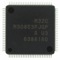
M30853FJGP#U3 Renesas Electronics America, M30853FJGP#U3 Datasheet - Page 30

M30853FJGP#U3
Manufacturer Part Number
M30853FJGP#U3
Description
IC M32C MCU FLASH 100LQFP
Manufacturer
Renesas Electronics America
Series
M16C™ M32C/80r
Datasheets
1.M3087BFLGPU3.pdf
(364 pages)
2.M30853FHFPD5.pdf
(94 pages)
3.M30853FHFPU3.pdf
(544 pages)
Specifications of M30853FJGP#U3
Core Processor
M32C/80
Core Size
16/32-Bit
Speed
32MHz
Connectivity
CAN, I²C, IEBus, SIO, UART/USART
Peripherals
DMA, WDT
Number Of I /o
85
Program Memory Size
512KB (512K x 8)
Program Memory Type
FLASH
Ram Size
24K x 8
Voltage - Supply (vcc/vdd)
3 V ~ 5.5 V
Data Converters
A/D 26x10b; D/A 2x8b
Oscillator Type
Internal
Operating Temperature
-40°C ~ 85°C
Package / Case
100-LQFP
For Use With
R0K330879S001BE - KIT DEV RSK M32C/87R0K330879S000BE - KIT DEV RSK M32C/87
Lead Free Status / RoHS Status
Lead free / RoHS Compliant
Eeprom Size
-
Available stocks
Company
Part Number
Manufacturer
Quantity
Price
Part Number:
M30853FJGP#U3M30853FJGP#D5
Manufacturer:
Renesas Electronics America
Quantity:
10 000
- Current page: 30 of 364
- Download datasheet (3Mb)
R
R
e
E
v
J
Chapter 1 Overview
Figure 1.7.3 Register bit specification
Figure 1.7.4 Addressing modes used for memory bit specification
Table 1.7.1 Bit-Specifying Address Range
1 .
0
1.7.3 Bits
(1) Register bits
(2) Memory bits
bit,base:19
bit,base:27
bit,base:11[SB]
bit,base:19[SB]
bit,base:11[FB]
bit,base:19[FB]
bit,[An]
bit,base:11[An]
bit,base:19[An]
bit,base:27[An]
9
0 .
Addressing
B
Figure 1.7.3 shows register bit specification.
Register bits can be specified by register direct (bit,RnH/RnL or bit,An). Use bit,RnH/RnL to specify
a bit in data register (RnH/RnL); use bit,An to specify a bit in address register (An).
For bit in bit,RnH/RnL and bit,An, you can specify a bit number in the range of 0 to 7.
Figure 1.7.4 shows addressing modes used for memory bit specification. Table 1.7.1 lists the address
range in which you can specify bits in each addressing mode. Be sure to observe the address range in
Table 1.7.1 when specifying memory bits.
0
0
3
1
2
9
0
Addressing mode
0 -
0
6
1
0 .
bit,RnH/RnL
(bit:0 to 7, n:0,1)
0
0
5
3 .
1
p
a
000000
g
Lower limit (address)
000000
000000
[SB]
[FB]-000080
[FB]-008000
[An]
[An]
[SB]
[An]
e
b7
12
RnH/RnL
16
16
16
Specification range
f o
Absolute addressing
SB-based relative addressing
FB-based relative addressing
Address register-based indirect
addressing
Address register-based relative
addressing
3
3
16
16
5
b0
Upper limit (address)
00FFFF
FFFFFF
[SB]+000FF
[SB]+0FFFF
[FB]+00007F
[FB]+007FFF
FFFFFF
[An]+0000FF
[An]+00FFFF
[An]+FFFFFF
bit,An
(bit:0 to 7, n:0,1)
16
16
16
16
16
16
16
16
16
b7
16
An
000000
000000
000000
000000
000000
000000
000000
b0
16
16
16
16
16
16
16
bit,base:19
bit,base:27
bit,base:19[SB]
bit,[An]
bit,base:11[SB]
bit,base:11[FB]
bit,base:19[FB]
bit,base:11[An]
bit,base:19[An]
bit,base:27[An]
The access range
to FFFFFF
to FFFFFF
to FFFFFF
to FFFFFF
to FFFFFF
to FFFFFF
to FFFFFF
16
16
16
16
16
16
16
.
.
.
.
.
.
.
1.7 Data Types
Related parts for M30853FJGP#U3
Image
Part Number
Description
Manufacturer
Datasheet
Request
R

Part Number:
Description:
KIT STARTER FOR M16C/29
Manufacturer:
Renesas Electronics America
Datasheet:

Part Number:
Description:
KIT STARTER FOR R8C/2D
Manufacturer:
Renesas Electronics America
Datasheet:

Part Number:
Description:
R0K33062P STARTER KIT
Manufacturer:
Renesas Electronics America
Datasheet:

Part Number:
Description:
KIT STARTER FOR R8C/23 E8A
Manufacturer:
Renesas Electronics America
Datasheet:

Part Number:
Description:
KIT STARTER FOR R8C/25
Manufacturer:
Renesas Electronics America
Datasheet:

Part Number:
Description:
KIT STARTER H8S2456 SHARPE DSPLY
Manufacturer:
Renesas Electronics America
Datasheet:

Part Number:
Description:
KIT STARTER FOR R8C38C
Manufacturer:
Renesas Electronics America
Datasheet:

Part Number:
Description:
KIT STARTER FOR R8C35C
Manufacturer:
Renesas Electronics America
Datasheet:

Part Number:
Description:
KIT STARTER FOR R8CL3AC+LCD APPS
Manufacturer:
Renesas Electronics America
Datasheet:

Part Number:
Description:
KIT STARTER FOR RX610
Manufacturer:
Renesas Electronics America
Datasheet:

Part Number:
Description:
KIT STARTER FOR R32C/118
Manufacturer:
Renesas Electronics America
Datasheet:

Part Number:
Description:
KIT DEV RSK-R8C/26-29
Manufacturer:
Renesas Electronics America
Datasheet:

Part Number:
Description:
KIT STARTER FOR SH7124
Manufacturer:
Renesas Electronics America
Datasheet:

Part Number:
Description:
KIT STARTER FOR H8SX/1622
Manufacturer:
Renesas Electronics America
Datasheet:

Part Number:
Description:
KIT DEV FOR SH7203
Manufacturer:
Renesas Electronics America
Datasheet:


