M30833FJGP#U3 Renesas Electronics America, M30833FJGP#U3 Datasheet - Page 12
M30833FJGP#U3
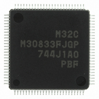
Manufacturer Part Number
M30833FJGP#U3
Description
IC M32C/83 MCU FLASH 100LQFP
Manufacturer
Renesas Electronics America
Series
M16C™ M32C/80r
Datasheets
1.M3087BFLGPU3.pdf
(364 pages)
2.M30833FJGPU3.pdf
(96 pages)
3.M30833FJGPU3.pdf
(529 pages)
Specifications of M30833FJGP#U3
Core Processor
M32C/80
Core Size
16/32-Bit
Speed
32MHz
Connectivity
CAN, I²C, IEBus, SIO, UART/USART
Peripherals
DMA, WDT
Number Of I /o
85
Program Memory Size
512KB (512K x 8)
Program Memory Type
FLASH
Ram Size
31K x 8
Voltage - Supply (vcc/vdd)
3 V ~ 5.5 V
Data Converters
A/D 26x10b; D/A 2x8b
Oscillator Type
Internal
Operating Temperature
-40°C ~ 85°C
Package / Case
100-LQFP
Package
100LQFP
Family Name
R8C
Maximum Speed
32 MHz
Operating Supply Voltage
5 V
Data Bus Width
16 Bit
Number Of Programmable I/os
87
Interface Type
UART
On-chip Adc
26-chx10-bit
On-chip Dac
2-chx8-bit
Number Of Timers
11
For Use With
R0K330879S001BE - KIT DEV RSK M32C/87R0K330879S000BE - KIT DEV RSK M32C/87
Lead Free Status / RoHS Status
Lead free / RoHS Compliant
Eeprom Size
-
Available stocks
Company
Part Number
Manufacturer
Quantity
Price


18. D/A Converter ______________________________ 240
19. CRC Calculation ____________________________ 243
20. X/Y Conversion _____________________________ 245
21. Intelligent I/O_______________________________ 248
22. CAN Module _______________________________ 324
A-6
21.1 Base Timer ............................................................................................................ 264
21.2 Time Measurement Function (Group 0 and 1) ................................................... 269
21.3 Waveform Generation Function .......................................................................... 274
21.4 Communication Unit 0 and 1 Communication Function .................................. 289
21.5 Group 2 Communication Function ..................................................................... 306
21.6 Group 3 Communication Function ..................................................................... 317
22.1 CAN-Associated Registers .................................................................................. 326
22.1.1 CAN0 Control Register 0 (C0CTLR0 Register) ............................................... 326
21.3.1 Single-Phase Waveform Output Mode (Group 0 to 3) ............................... 276
21.3.2 Phase-Delayed Waveform Output Mode (Group 0 to 3) ............................ 278
21.3.3 Set/Reset Waveform Output (SR Waveform Output) Mode (Group 0 to 3) .... 280
21.3.4 Bit Modulation PWM Output Mode (Group 2 and 3) .................................. 283
21.3.5 Real-Time Port (RTP) Output Mode (Group 2 and 3) ................................. 285
21.3.6 Parallel Real-Time Port Output Mode (Group 2 and 3) .............................. 287
21.4.1 Clock Synchronous Serial I/O Mode (Groups 0 and 1) .............................. 296
21.4.2 Clock Asynchronous Serial I/O Mode (UART) (Groups 0 and 1) .............. 299
21.4.3 HDLC Data Processing Mode (Group 0 and 1) ........................................... 303
21.5.1 Variable Clock Synchronous Serial I/O Mode (Group 2) ........................... 310
21.5.2 IEBus Mode (Group 2) .................................................................................. 314
21.6.1 8-bit or 16-bit Clock Synchronous Serial I/O Mode (Group 3) .................. 320
22.1.2 CAN0 Control Register 1 (C0CTLR1 Register) ........................................... 329
22.1.3 CAN0 Sleep Control Register (C0SLPR Register) ..................................... 330
22.1.4 CAN0 Status Register (C0STR Register) .................................................... 331
22.1.5 CAN0 Extended ID Register (C0IDR Register) ........................................... 333
22.1.6 CAN0 Configuration Register (C0CONR Register) .................................... 334
22.1.8 CAN0 Transmit Error Count Register (C0TEC Register) ........................... 336
22.1.7 CAN0 Time Stamp Register (C0TSR Register) ........................................... 336
22.1.9 CAN0 Receive Error Count Register (C0REC Register) ............................ 337
22.1.10 CAN0 Baud Rate Prescaler (C0BRP Register) ......................................... 337
22.1.11 CAN0 Slot Interrupt Status Register (C0SISTR Register) ....................... 338
22.1.12 CAN0 Slot Interrupt Mask Register (C0SIMKR Register) ........................ 340
Related parts for M30833FJGP#U3
Image
Part Number
Description
Manufacturer
Datasheet
Request
R

Part Number:
Description:
KIT STARTER FOR M16C/29
Manufacturer:
Renesas Electronics America
Datasheet:

Part Number:
Description:
KIT STARTER FOR R8C/2D
Manufacturer:
Renesas Electronics America
Datasheet:

Part Number:
Description:
R0K33062P STARTER KIT
Manufacturer:
Renesas Electronics America
Datasheet:

Part Number:
Description:
KIT STARTER FOR R8C/23 E8A
Manufacturer:
Renesas Electronics America
Datasheet:

Part Number:
Description:
KIT STARTER FOR R8C/25
Manufacturer:
Renesas Electronics America
Datasheet:

Part Number:
Description:
KIT STARTER H8S2456 SHARPE DSPLY
Manufacturer:
Renesas Electronics America
Datasheet:

Part Number:
Description:
KIT STARTER FOR R8C38C
Manufacturer:
Renesas Electronics America
Datasheet:

Part Number:
Description:
KIT STARTER FOR R8C35C
Manufacturer:
Renesas Electronics America
Datasheet:

Part Number:
Description:
KIT STARTER FOR R8CL3AC+LCD APPS
Manufacturer:
Renesas Electronics America
Datasheet:
Part Number:
Description:
KIT STARTER FOR RX610
Manufacturer:
Renesas Electronics America
Datasheet:

Part Number:
Description:
KIT STARTER FOR R32C/118
Manufacturer:
Renesas Electronics America
Datasheet:

Part Number:
Description:
KIT DEV RSK-R8C/26-29
Manufacturer:
Renesas Electronics America
Datasheet:

Part Number:
Description:
KIT STARTER FOR SH7124
Manufacturer:
Renesas Electronics America
Datasheet:

Part Number:
Description:
KIT STARTER FOR H8SX/1622
Manufacturer:
Renesas Electronics America
Datasheet:

Part Number:
Description:
KIT DEV FOR SH7203
Manufacturer:
Renesas Electronics America
Datasheet: