M30833FJGP#U3 Renesas Electronics America, M30833FJGP#U3 Datasheet - Page 518
M30833FJGP#U3
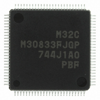
Manufacturer Part Number
M30833FJGP#U3
Description
IC M32C/83 MCU FLASH 100LQFP
Manufacturer
Renesas Electronics America
Series
M16C™ M32C/80r
Datasheets
1.M3087BFLGPU3.pdf
(364 pages)
2.M30833FJGPU3.pdf
(96 pages)
3.M30833FJGPU3.pdf
(529 pages)
Specifications of M30833FJGP#U3
Core Processor
M32C/80
Core Size
16/32-Bit
Speed
32MHz
Connectivity
CAN, I²C, IEBus, SIO, UART/USART
Peripherals
DMA, WDT
Number Of I /o
85
Program Memory Size
512KB (512K x 8)
Program Memory Type
FLASH
Ram Size
31K x 8
Voltage - Supply (vcc/vdd)
3 V ~ 5.5 V
Data Converters
A/D 26x10b; D/A 2x8b
Oscillator Type
Internal
Operating Temperature
-40°C ~ 85°C
Package / Case
100-LQFP
Package
100LQFP
Family Name
R8C
Maximum Speed
32 MHz
Operating Supply Voltage
5 V
Data Bus Width
16 Bit
Number Of Programmable I/os
87
Interface Type
UART
On-chip Adc
26-chx10-bit
On-chip Dac
2-chx8-bit
Number Of Timers
11
For Use With
R0K330879S001BE - KIT DEV RSK M32C/87R0K330879S000BE - KIT DEV RSK M32C/87
Lead Free Status / RoHS Status
Lead free / RoHS Compliant
Eeprom Size
-
Available stocks
Company
Part Number
Manufacturer
Quantity
Price


Rev.
REVISION HISTORY
Date
Page
103
104
106
55
60
64
65
67
68
69
72
75
77
79
80
81
84
85
86
87
88
93
95
99
Bus
• 7.1.3.2 Multiplexed Bus revised
• 7.2.4 Bus Timing revised
• 7.6 RDY Signal revised
• Figure 7.7 RD Signal Output Extended by RDY Signal modified
Clock Generating Circuit
Chapter name changed from “System Clock “ to “Clock Generating Circuit”
• Table 8.1 Clock Generation Circuit Specifications
• Figure 8.1 Clock Generation Circuit revised
• Figure 8.5 CM2 Register CM21 bit function modified; Note 5 revised
• Figure 8.8 PLC1 Register Note 3 revised; Note 4 added
• 8.1.2 Sub Clock revised
• Figure 8.11 Switching Procedure form On-chip Oscillator Clock to Main
• 8.1.4 PLL Clock revised
• Table 8.2 Bit Settings to Use PLL Clock as CPU Clock Source Setting added
• Figure 8.13 Procedure to Use PLL Clock as CPU Clock Source modified
• 8.2 CPU Clock and BCLK revised
• 8.5.2.2 Before Entering Wait Mode revised
• 8.5.2.5 Entering Wait Mode added
• 8.5.3 Stop Mode revised
• 8.5.3.1 Before Entering Stop Mode revised
• 8.5.3.3 Exiting Stop Mode revised
• 8.5.3.4 Entering Stop Mode added
• Figure 8.15 Status Transition modified
Interrupts
• Table 10.1 Fixed Vector Table Point of reference changed
• Table 10.2 Relocatable Vector Tables Reserved Space added
• 10.6.2.3 RLVL2 to RLVL0 Bits revised
• Figure 10.8 Interrupt Priority “Oscillation Stop Detect” added
• Figure 10.9 Interrupt Priority Level Select Circuit modified
• 10.8 NMI Interrupt revised
• Figure 8.2 CM0 Register Bit 3 function changed from “Nothing is assigned” to
• Figure 10.5 RLVL Register Value after reset changed; Note 3 revised; Note 4
Main clock clock frequency modified; “Ceramic oscillator” changed to “Ceramic
resonator”; Reference point added to PLL Frequency Synthesizer
“Reserved Bit”
Clock modified
for when f(X
added
________
M32C/83 GROUP (M32C/83, M32C/83T) Hardware Manual
_____
IN
) is 8MHz
C-5
Description
Summary
________
Related parts for M30833FJGP#U3
Image
Part Number
Description
Manufacturer
Datasheet
Request
R

Part Number:
Description:
KIT STARTER FOR M16C/29
Manufacturer:
Renesas Electronics America
Datasheet:

Part Number:
Description:
KIT STARTER FOR R8C/2D
Manufacturer:
Renesas Electronics America
Datasheet:

Part Number:
Description:
R0K33062P STARTER KIT
Manufacturer:
Renesas Electronics America
Datasheet:

Part Number:
Description:
KIT STARTER FOR R8C/23 E8A
Manufacturer:
Renesas Electronics America
Datasheet:

Part Number:
Description:
KIT STARTER FOR R8C/25
Manufacturer:
Renesas Electronics America
Datasheet:

Part Number:
Description:
KIT STARTER H8S2456 SHARPE DSPLY
Manufacturer:
Renesas Electronics America
Datasheet:

Part Number:
Description:
KIT STARTER FOR R8C38C
Manufacturer:
Renesas Electronics America
Datasheet:

Part Number:
Description:
KIT STARTER FOR R8C35C
Manufacturer:
Renesas Electronics America
Datasheet:

Part Number:
Description:
KIT STARTER FOR R8CL3AC+LCD APPS
Manufacturer:
Renesas Electronics America
Datasheet:
Part Number:
Description:
KIT STARTER FOR RX610
Manufacturer:
Renesas Electronics America
Datasheet:

Part Number:
Description:
KIT STARTER FOR R32C/118
Manufacturer:
Renesas Electronics America
Datasheet:

Part Number:
Description:
KIT DEV RSK-R8C/26-29
Manufacturer:
Renesas Electronics America
Datasheet:

Part Number:
Description:
KIT STARTER FOR SH7124
Manufacturer:
Renesas Electronics America
Datasheet:

Part Number:
Description:
KIT STARTER FOR H8SX/1622
Manufacturer:
Renesas Electronics America
Datasheet:

Part Number:
Description:
KIT DEV FOR SH7203
Manufacturer:
Renesas Electronics America
Datasheet: