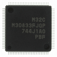
M30833FJGP#U3 Renesas Electronics America, M30833FJGP#U3 Datasheet - Page 130

M30833FJGP#U3
Manufacturer Part Number
M30833FJGP#U3
Description
IC M32C/83 MCU FLASH 100LQFP
Manufacturer
Renesas Electronics America
Series
M16C™ M32C/80r
Datasheets
1.M3087BFLGPU3.pdf
(364 pages)
2.M30833FJGPU3.pdf
(96 pages)
3.M30833FJGPU3.pdf
(529 pages)
Specifications of M30833FJGP#U3
Core Processor
M32C/80
Core Size
16/32-Bit
Speed
32MHz
Connectivity
CAN, I²C, IEBus, SIO, UART/USART
Peripherals
DMA, WDT
Number Of I /o
85
Program Memory Size
512KB (512K x 8)
Program Memory Type
FLASH
Ram Size
31K x 8
Voltage - Supply (vcc/vdd)
3 V ~ 5.5 V
Data Converters
A/D 26x10b; D/A 2x8b
Oscillator Type
Internal
Operating Temperature
-40°C ~ 85°C
Package / Case
100-LQFP
Package
100LQFP
Family Name
R8C
Maximum Speed
32 MHz
Operating Supply Voltage
5 V
Data Bus Width
16 Bit
Number Of Programmable I/os
87
Interface Type
UART
On-chip Adc
26-chx10-bit
On-chip Dac
2-chx8-bit
Number Of Timers
11
For Use With
R0K330879S001BE - KIT DEV RSK M32C/87R0K330879S000BE - KIT DEV RSK M32C/87
Lead Free Status / RoHS Status
Lead free / RoHS Compliant
Eeprom Size
-
Available stocks
Company
Part Number
Manufacturer
Quantity
Price
- Current page: 130 of 529
- Download datasheet (5Mb)
R
R
M
10.7 INT Interrupt
e
E
3
. v
J
Figure 10.10 IFSR Register
2
0
External input generates the INTi interrupt (i = 0 to 5). The LVS bit in the INTiIC register selects either edge
sensitive triggering to generate an interrupt on any edge or level sensitive triggering to generate an inter-
rupt at an applied signal level. The POL bit in the INTiIC register determines the polarity.
With an edge sensitive triggering, when the IFSRi bit in the IFSR register is set to "1" (both edges), an
interrupt occurs on both rising and falling edges of the external input. If the IFSRi bit is set to "1", set the
POL bit in the corresponding register to "0" (falling edge).
With a level sensitive triggering, set the IFSRi bit to "0" (single edge). When the INTi pin input level reaches
the level set in the POL bit, the IR bit in the INTiIC register is set to "1". The IR bit remains set to "1" even
if the INTi pin level is changed. The IR bit is set to "0" when the INTi interrupt is acknowledged or when "0"
is written by program.
Figure 10.10 shows the IFSR register.
1
C
9
3 .
B
8 /
0
1
______
3
0
3
_______
J
G
4
a
0 -
n
o r
External Interrupt Request Cause Select Register
b7
3 .
1
NOTES:
u
, 1
3
p
b6
1
1.Set this bit to "0" to select level sensitive.
2
(
M
0
b5
When setting this bit to "1", set the POL bit in the INTilC register (i = 0 to 5) to "0" (falling edge).
0
3
6
2
b4
C
8 /
Page 105
b3
, 3
b2
M
b1
3
2
b0
C
______
f o
8 /
4
3
Symbol
IFSR7
IFSR6
8
IFSR0
IFSR2
IFSR4
IFSR5
IFSR1
IFSR3
) T
8
Bit
Symbol
IFSR
INT0 Interrupt Polarity
Select Bit
INT1 Interrupt Polarity
Select Bit
INT2 Interrupt Polarity
Select Bit
INT3 Interrupt Polarity
Select Bit
INT4 Interrupt Polarity
Select Bit
INT5 Interrupt Polarity
Select Bit
UART0, UART3
Interrupt Cause Select
Bit
UART1, UART4
Interrupt Cause Select
Bit
Bit Name
(1)
(1)
(1)
(1)
(1)
(1)
Address
031F
16
0 : UART3 bus conflict, start condition
1 : UART0 bus conflict, start condition
0 : UART4 bus conflict, start condition
1 : UART1 bus conflict, start condition
0 : One edge
1 : Both edges
0 : One edge
1 : Both edges
0 : One edge
1 : Both edges
0 : One edge
1 : Both edges
0 : One edge
1 : Both edges
0 : One edge
1 : Both edges
_______
detect, stop condition detect, fault
error detect
detect, stop condition detect, fault
error detect
detect, stop condition detect, fault
error detect
detect, stop condition detect, fault
error detect
Function
After Reset
00
16
_______
RW
RW
RW
RW
RW
RW
RW
RW
RW
10. Interrupts
Related parts for M30833FJGP#U3
Image
Part Number
Description
Manufacturer
Datasheet
Request
R

Part Number:
Description:
KIT STARTER FOR M16C/29
Manufacturer:
Renesas Electronics America
Datasheet:

Part Number:
Description:
KIT STARTER FOR R8C/2D
Manufacturer:
Renesas Electronics America
Datasheet:

Part Number:
Description:
R0K33062P STARTER KIT
Manufacturer:
Renesas Electronics America
Datasheet:

Part Number:
Description:
KIT STARTER FOR R8C/23 E8A
Manufacturer:
Renesas Electronics America
Datasheet:

Part Number:
Description:
KIT STARTER FOR R8C/25
Manufacturer:
Renesas Electronics America
Datasheet:

Part Number:
Description:
KIT STARTER H8S2456 SHARPE DSPLY
Manufacturer:
Renesas Electronics America
Datasheet:

Part Number:
Description:
KIT STARTER FOR R8C38C
Manufacturer:
Renesas Electronics America
Datasheet:

Part Number:
Description:
KIT STARTER FOR R8C35C
Manufacturer:
Renesas Electronics America
Datasheet:

Part Number:
Description:
KIT STARTER FOR R8CL3AC+LCD APPS
Manufacturer:
Renesas Electronics America
Datasheet:

Part Number:
Description:
KIT STARTER FOR RX610
Manufacturer:
Renesas Electronics America
Datasheet:

Part Number:
Description:
KIT STARTER FOR R32C/118
Manufacturer:
Renesas Electronics America
Datasheet:

Part Number:
Description:
KIT DEV RSK-R8C/26-29
Manufacturer:
Renesas Electronics America
Datasheet:

Part Number:
Description:
KIT STARTER FOR SH7124
Manufacturer:
Renesas Electronics America
Datasheet:

Part Number:
Description:
KIT STARTER FOR H8SX/1622
Manufacturer:
Renesas Electronics America
Datasheet:

Part Number:
Description:
KIT DEV FOR SH7203
Manufacturer:
Renesas Electronics America
Datasheet:


