R5F21191SP#U0 Renesas Electronics America, R5F21191SP#U0 Datasheet - Page 17
R5F21191SP#U0
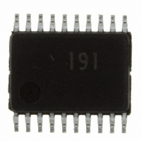
Manufacturer Part Number
R5F21191SP#U0
Description
IC R8C MCU FLASH 8K 20SSOP
Manufacturer
Renesas Electronics America
Series
M16C™ M16C/R8C/Tiny/19r
Datasheets
1.R5F211A2SPU0.pdf
(300 pages)
2.R5F21181DSPU0.pdf
(43 pages)
3.R5F21181DSPU0.pdf
(259 pages)
Specifications of R5F21191SP#U0
Core Processor
R8C
Core Size
16-Bit
Speed
20MHz
Connectivity
SIO, UART/USART
Peripherals
LED, POR, Voltage Detect, WDT
Number Of I /o
13
Program Memory Size
4KB (4K x 8)
Program Memory Type
FLASH
Ram Size
384 x 8
Voltage - Supply (vcc/vdd)
2.7 V ~ 5.5 V
Data Converters
A/D 4x1b
Oscillator Type
Internal
Operating Temperature
-20°C ~ 85°C
Package / Case
20-SSOP
For Use With
R0K521134S000BE - KIT EVAL STARTER FOR R8C/13R0E521174CPE10 - EMULATOR COMPACT R8C/18/19/1
Lead Free Status / RoHS Status
Lead free / RoHS Compliant
Eeprom Size
-


NOTE:
Address
0080h
0081h
0082h
0083h
0084h
0085h
0086h
0087h
0088h
0089h
008Ah
008Bh
008Ch
008Dh
008Eh
008Fh
0090h
0091h
0092h
0093h
0094h
0095h
0096h
0097h
0098h
0099h
009Ah
009Bh
009Ch
009Dh
009Eh
009Fh
00A0h
00A1h
00A2h
00A3h
00A4h
00A5h
00A6h
00A7h
00A8h
00A9h
00AAh
00ABh
00ACh
00ADh
00AEh
00AFh
00B0h
00B1h
00B2h
00B3h
00B4h
00B5h
00B6h
00B7h
00B8h
00B9h
00BAh
00BBh
00BCh
00BDh
00BEh
00BFh
1. The blank regions, 0100h to 01AFh, and 01C0h to 02FFh
are reserved. Do not access locations in these regions.
Register
Timer Z Mode Register
Timer Z Waveform Output Control Register
Prescaler Z Register
Timer Z Secondary Register
Timer Z Primary Register
Timer Z Output Control Register
Timer X Mode Register
Prescaler X Register
Timer X Register
Timer Count Source Set Register
Timer C Register
External Input Enable Register
Key Input Enable Register
Timer C Control Register 0
Timer C Control Register 1
Capture, Compare 0 Register
Compare 1 Register
UART0 Transmit/Receive Mode Register
UART0 Bit Rate Register
UART0 Transmit Buffer Register
UART0 Transmit/Receive Control Register 0
UART0 Transmit/Receive Control Register 1
UART0 Receive Buffer Register
UART1 Transmit/Receive Mode Register
UART1 Bit Rate Register
UART1 Transmit Buffer Register
UART1 Transmit/Receive Control Register 0
UART1 Transmit/Receive Control Register 1
UART1 Receive Buffer Register
UART Transmit/Receive Control Register 2
Symbol
TZMR
PUM
PREZ
TZSC
TZPR
TZOC
TXMR
PREX
TX
TCSS
TC
INTEN
KIEN
TCC0
TCC1
TM0
TM1
U0MR
U0BRG
U0TB
U0C0
U0C1
U0RB
U1MR
U1BRG
U1TB
U1C0
U1C1
U1RB
UCON
105,121
Page
120
120
104
105
105
137
138
139
137
137
149
148
148
150
151
148
149
148
148
150
151
148
151
118
119
119
119
85
91
B - 2
Address
00C0h
00C1h
00C2h
00C3h
00C4h
00C5h
00C6h
00C7h
00C8h
00C9h
00CAh
00CBh
00CCh
00CDh
00CEh
00CFh
00D0h
00D1h
00D2h
00D3h
00D4h
00D5h
00D6h
00D7h
00D8h
00D9h
00DAh
00DBh
00DCh
00DDh
00DEh
00DFh
00E0h
00E1h
00E2h
00E3h
00E4h
00E5h
00E6h
00E7h
00E8h
00E9h
00EAh
00EBh
00ECh
00EDh
00EEh
00EFh
00F0h
00F1h
00F2h
00F3h
00F4h
00F5h
00F6h
00F7h
00F8h
00F9h
00FAh
00FBh
00FCh
00FDh
00FEh
00FFh
01B3h
01B4h
01B5h
01B6h
01B7h
0FFFFh
Register
A/D Register
A/D Control Register 2
A/D Control Register 0
A/D Control Register 1
Port P1 Register
Port P1 Direction Register
Port P3 Register
Port P3 Direction Register
Port P4 Register
Port P4 Direction Register
Pull-Up Control Register 0
Pull-Up Control Register 1
Port P1 Drive Capacity Control Register
Timer C Output Control Register
Flash Memory Control Register 4
Flash Memory Control Register 1
Flash Memory Control Register 0
Optional Function Select Register
Symbol
AD
ADCON2
ADCON0
ADCON1
P1
PD1
P3
PD3
P4
PD4
PUR0
PUR1
DRR
TCOUT
FMR4
FMR1
FMR0
OFS
98,177
Page
166
166
165
165
140
184
183
182
33
33
33
33
33
33
34
34
34
Related parts for R5F21191SP#U0
Image
Part Number
Description
Manufacturer
Datasheet
Request
R

Part Number:
Description:
KIT STARTER FOR M16C/29
Manufacturer:
Renesas Electronics America
Datasheet:

Part Number:
Description:
KIT STARTER FOR R8C/2D
Manufacturer:
Renesas Electronics America
Datasheet:

Part Number:
Description:
R0K33062P STARTER KIT
Manufacturer:
Renesas Electronics America
Datasheet:

Part Number:
Description:
KIT STARTER FOR R8C/23 E8A
Manufacturer:
Renesas Electronics America
Datasheet:

Part Number:
Description:
KIT STARTER FOR R8C/25
Manufacturer:
Renesas Electronics America
Datasheet:

Part Number:
Description:
KIT STARTER H8S2456 SHARPE DSPLY
Manufacturer:
Renesas Electronics America
Datasheet:

Part Number:
Description:
KIT STARTER FOR R8C38C
Manufacturer:
Renesas Electronics America
Datasheet:

Part Number:
Description:
KIT STARTER FOR R8C35C
Manufacturer:
Renesas Electronics America
Datasheet:

Part Number:
Description:
KIT STARTER FOR R8CL3AC+LCD APPS
Manufacturer:
Renesas Electronics America
Datasheet:
Part Number:
Description:
KIT STARTER FOR RX610
Manufacturer:
Renesas Electronics America
Datasheet:

Part Number:
Description:
KIT STARTER FOR R32C/118
Manufacturer:
Renesas Electronics America
Datasheet:

Part Number:
Description:
KIT DEV RSK-R8C/26-29
Manufacturer:
Renesas Electronics America
Datasheet:

Part Number:
Description:
KIT STARTER FOR SH7124
Manufacturer:
Renesas Electronics America
Datasheet:

Part Number:
Description:
KIT STARTER FOR H8SX/1622
Manufacturer:
Renesas Electronics America
Datasheet:

Part Number:
Description:
KIT DEV FOR SH7203
Manufacturer:
Renesas Electronics America
Datasheet: