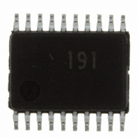
R5F21191SP#U0 Renesas Electronics America, R5F21191SP#U0 Datasheet - Page 172

R5F21191SP#U0
Manufacturer Part Number
R5F21191SP#U0
Description
IC R8C MCU FLASH 8K 20SSOP
Manufacturer
Renesas Electronics America
Series
M16C™ M16C/R8C/Tiny/19r
Datasheets
1.R5F211A2SPU0.pdf
(300 pages)
2.R5F21181DSPU0.pdf
(43 pages)
3.R5F21181DSPU0.pdf
(259 pages)
Specifications of R5F21191SP#U0
Core Processor
R8C
Core Size
16-Bit
Speed
20MHz
Connectivity
SIO, UART/USART
Peripherals
LED, POR, Voltage Detect, WDT
Number Of I /o
13
Program Memory Size
4KB (4K x 8)
Program Memory Type
FLASH
Ram Size
384 x 8
Voltage - Supply (vcc/vdd)
2.7 V ~ 5.5 V
Data Converters
A/D 4x1b
Oscillator Type
Internal
Operating Temperature
-20°C ~ 85°C
Package / Case
20-SSOP
For Use With
R0K521134S000BE - KIT EVAL STARTER FOR R8C/13R0E521174CPE10 - EMULATOR COMPACT R8C/18/19/1
Lead Free Status / RoHS Status
Lead free / RoHS Compliant
Eeprom Size
-
- Current page: 172 of 259
- Download datasheet (3Mb)
R8C/18 Group, R8C/19 Group
Rev.1.30
REJ09B0222-0130
Figure 15.8
Figure 15.9
15.1.1
15.1.2
transfer clock polarity.
Figure 15.9 shows the Transfer Format. Use the UFORM bit in the U0C0 register to select the
transfer format.
Figure 15.8 shows the Transfer Clock Polarity. Use the CKPOL bit in the U0C0 register to select the
Apr 14, 2006
Polarity Select Function
LSB First/MSB First Select Function
• When UFORM bit in U0C0 register = 0 (LSB first)
• When UFORM bit in U0C0 register = 1 (MSB first)
NOTE:
RXD0
RXD0
CLK0
TXD0
CLK0
TXD0
Transfer Clock Polarity
Transfer Format
CLK0
CLK0
• When the CKPOL bit in the U0C0 register = 0 (output transmit data at the falling
• When the CKPOL bit in the U0C0 register = 1 (output transmit data at the rising
RXD0
RXD0
TXD0
TXD0
edge and input the receive data at the rising edge of the transfer clock)
edge and input receive data at the falling edge of the transfer clock)
NOTES:
1. When not transferring, the CLK0 pin level is “H”.
2. When not transferring, the CLK0 pin level is “L”.
1. The above applies when the CKPOL bit in the U0C0 register is
(1)
(2)
set to 0 (output transmit data at the falling edge and input receive
data at the rising edge of the transfer clock).
Page 155 of 233
D0
D0
D7
D7
D0
D0
D0
D0
D1
D1
D6
D6
D1
D1
D1
D1
D2
D2
D5
D5
D2
D2
D2
D2
D3
D3
D4
D4
D3
D3
D3
D3
D4
D4
D3
D3
(1)
(1)
D4
D4
D4
D4
D5
D5
D2
D2
D5
D5
D5
D5
D6
D6
D1
D1
D6
D6
D6
D6
D7
D7
D0
D0
D7
D7
D7
D7
15. Serial Interface
Related parts for R5F21191SP#U0
Image
Part Number
Description
Manufacturer
Datasheet
Request
R

Part Number:
Description:
KIT STARTER FOR M16C/29
Manufacturer:
Renesas Electronics America
Datasheet:

Part Number:
Description:
KIT STARTER FOR R8C/2D
Manufacturer:
Renesas Electronics America
Datasheet:

Part Number:
Description:
R0K33062P STARTER KIT
Manufacturer:
Renesas Electronics America
Datasheet:

Part Number:
Description:
KIT STARTER FOR R8C/23 E8A
Manufacturer:
Renesas Electronics America
Datasheet:

Part Number:
Description:
KIT STARTER FOR R8C/25
Manufacturer:
Renesas Electronics America
Datasheet:

Part Number:
Description:
KIT STARTER H8S2456 SHARPE DSPLY
Manufacturer:
Renesas Electronics America
Datasheet:

Part Number:
Description:
KIT STARTER FOR R8C38C
Manufacturer:
Renesas Electronics America
Datasheet:

Part Number:
Description:
KIT STARTER FOR R8C35C
Manufacturer:
Renesas Electronics America
Datasheet:

Part Number:
Description:
KIT STARTER FOR R8CL3AC+LCD APPS
Manufacturer:
Renesas Electronics America
Datasheet:

Part Number:
Description:
KIT STARTER FOR RX610
Manufacturer:
Renesas Electronics America
Datasheet:

Part Number:
Description:
KIT STARTER FOR R32C/118
Manufacturer:
Renesas Electronics America
Datasheet:

Part Number:
Description:
KIT DEV RSK-R8C/26-29
Manufacturer:
Renesas Electronics America
Datasheet:

Part Number:
Description:
KIT STARTER FOR SH7124
Manufacturer:
Renesas Electronics America
Datasheet:

Part Number:
Description:
KIT STARTER FOR H8SX/1622
Manufacturer:
Renesas Electronics America
Datasheet:

Part Number:
Description:
KIT DEV FOR SH7203
Manufacturer:
Renesas Electronics America
Datasheet:


