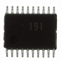
R5F21191SP#U0 Renesas Electronics America, R5F21191SP#U0 Datasheet - Page 193

R5F21191SP#U0
Manufacturer Part Number
R5F21191SP#U0
Description
IC R8C MCU FLASH 8K 20SSOP
Manufacturer
Renesas Electronics America
Series
M16C™ M16C/R8C/Tiny/19r
Datasheets
1.R5F211A2SPU0.pdf
(300 pages)
2.R5F21181DSPU0.pdf
(43 pages)
3.R5F21181DSPU0.pdf
(259 pages)
Specifications of R5F21191SP#U0
Core Processor
R8C
Core Size
16-Bit
Speed
20MHz
Connectivity
SIO, UART/USART
Peripherals
LED, POR, Voltage Detect, WDT
Number Of I /o
13
Program Memory Size
4KB (4K x 8)
Program Memory Type
FLASH
Ram Size
384 x 8
Voltage - Supply (vcc/vdd)
2.7 V ~ 5.5 V
Data Converters
A/D 4x1b
Oscillator Type
Internal
Operating Temperature
-20°C ~ 85°C
Package / Case
20-SSOP
For Use With
R0K521134S000BE - KIT EVAL STARTER FOR R8C/13R0E521174CPE10 - EMULATOR COMPACT R8C/18/19/1
Lead Free Status / RoHS Status
Lead free / RoHS Compliant
Eeprom Size
-
- Current page: 193 of 259
- Download datasheet (3Mb)
R8C/18 Group, R8C/19 Group
Rev.1.30
REJ09B0222-0130
17.3
Figure 17.3
17.3.1
Standard serial I/O mode has an ID code check function, and parallel I/O mode has a ROM code protect
function to prevent the flash memory from being read or rewritten easily.
This function is used in standard serial I/O mode. Unless the flash memory is blank, the ID codes sent
from the programmer and the ID codes written in the flash memory are checked to see if they match.
If the ID codes do not match, the commands sent from the programmer are not acknowledged. The
ID codes consist of 8 bits of data each, the areas of which, beginning with the first byte, are 00FFDFh,
00FFE3h, 00FFEBh, 00FFEFh, 00FFF3h, 00FFF7h, and 00FFFBh. Write programs in which the ID
codes are set at these addresses and write them to the flash memory.
Functions to Prevent Rewriting of Flash Memory
Apr 14, 2006
ID Code Check Function
Address for Stored ID Code
Page 176 of 233
00FFDFh to 00FFDCh
00FFE3h to 00FFE0h
00FFE7h to 00FFE4h
00FFEBh to 00FFE8h
00FFEFh to 00FFECh
00FFF3h to 00FFF0h
00FFF7h to 00FFF4h
00FFFBh to 00FFF8h
00FFFFh to 00FFFCh
NOTE:
1. The OFS register is assigned to 00FFFFh. Refer to
Address
Figure 13.2 Registers OFS and WDC and Figure
13.3 Registers WDTR and WDTS for OFS register
details.
(Note 1)
ID1
ID2
ID3
ID4
ID5
ID6
ID7
Oscillation stop detection/watchdog
timer/voltage monitor 2 vector
Undefined instruction vector
Overflow vector
BRK instruction vector
Address match vector
Single step vector
Address break
Reset vector
4 bytes
(Reserved)
17. Flash Memory Version
Related parts for R5F21191SP#U0
Image
Part Number
Description
Manufacturer
Datasheet
Request
R

Part Number:
Description:
KIT STARTER FOR M16C/29
Manufacturer:
Renesas Electronics America
Datasheet:

Part Number:
Description:
KIT STARTER FOR R8C/2D
Manufacturer:
Renesas Electronics America
Datasheet:

Part Number:
Description:
R0K33062P STARTER KIT
Manufacturer:
Renesas Electronics America
Datasheet:

Part Number:
Description:
KIT STARTER FOR R8C/23 E8A
Manufacturer:
Renesas Electronics America
Datasheet:

Part Number:
Description:
KIT STARTER FOR R8C/25
Manufacturer:
Renesas Electronics America
Datasheet:

Part Number:
Description:
KIT STARTER H8S2456 SHARPE DSPLY
Manufacturer:
Renesas Electronics America
Datasheet:

Part Number:
Description:
KIT STARTER FOR R8C38C
Manufacturer:
Renesas Electronics America
Datasheet:

Part Number:
Description:
KIT STARTER FOR R8C35C
Manufacturer:
Renesas Electronics America
Datasheet:

Part Number:
Description:
KIT STARTER FOR R8CL3AC+LCD APPS
Manufacturer:
Renesas Electronics America
Datasheet:

Part Number:
Description:
KIT STARTER FOR RX610
Manufacturer:
Renesas Electronics America
Datasheet:

Part Number:
Description:
KIT STARTER FOR R32C/118
Manufacturer:
Renesas Electronics America
Datasheet:

Part Number:
Description:
KIT DEV RSK-R8C/26-29
Manufacturer:
Renesas Electronics America
Datasheet:

Part Number:
Description:
KIT STARTER FOR SH7124
Manufacturer:
Renesas Electronics America
Datasheet:

Part Number:
Description:
KIT STARTER FOR H8SX/1622
Manufacturer:
Renesas Electronics America
Datasheet:

Part Number:
Description:
KIT DEV FOR SH7203
Manufacturer:
Renesas Electronics America
Datasheet:


