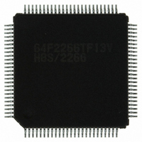
DF2266TF13V Renesas Electronics America, DF2266TF13V Datasheet - Page 163

DF2266TF13V
Manufacturer Part Number
DF2266TF13V
Description
IC H8S/2266 MCU FLASH 100-TQFP
Manufacturer
Renesas Electronics America
Series
H8® H8S/2200r
Datasheet
1.DF2266TF20V.pdf
(712 pages)
Specifications of DF2266TF13V
Core Processor
H8S/2000
Core Size
16-Bit
Speed
13MHz
Connectivity
I²C, SCI, SmartCard
Peripherals
LCD, POR, PWM, WDT
Number Of I /o
67
Program Memory Size
128KB (128K x 8)
Program Memory Type
FLASH
Ram Size
8K x 8
Voltage - Supply (vcc/vdd)
3 V ~ 5.5 V
Data Converters
A/D 10x10b
Oscillator Type
Internal
Operating Temperature
-20°C ~ 75°C
Package / Case
100-TQFP, 100-VQFP
Lead Free Status / RoHS Status
Lead free / RoHS Compliant
Eeprom Size
-
- Current page: 163 of 712
- Download datasheet (5Mb)
The H8S/2000 CPU is driven by a system clock, denoted by the symbol φ.
The bus controller controls a memory cycle and a bus cycle. Different methods are used to access
on-chip memory and on-chip peripheral modules. In the H8S/2268 Group, the bus controller also
has a bus arbitration function, and controls the operation of the internal bus masters: the CPU and
data transfer controller (DTC).
7.1
The period from one rising edge of φ to the next is referred to as a "state". The memory cycle or
bus cycle consists of one, two, or four states. Different methods are used to access on-chip
memory, on-chip peripheral modules, and the external address space.
7.1.1
On-chip memory is accessed in one state. The data bus is 16 bits wide, permitting both byte and
word transfer instruction. Figure 7.1 shows the on-chip memory access cycle.
Basic Timing
On-Chip Memory Access Timing (ROM, RAM)
Internal address bus
Read
access
Write
access
φ
Figure 7.1 On-Chip Memory Access Cycle
Internal read signal
Internal data bus
Internal write signal
Internal data bus
Section 7 Bus Controller
Bus cycle
Address
Rev. 5.00 Sep. 01, 2009 Page 111 of 656
T1
Read data
Write data
Section 7 Bus Controller
REJ09B0071-0500
Related parts for DF2266TF13V
Image
Part Number
Description
Manufacturer
Datasheet
Request
R

Part Number:
Description:
CONN SOCKET 2POS 7.92MM WHITE
Manufacturer:
Hirose Electric Co Ltd
Datasheet:

Part Number:
Description:
CONN SOCKET 4POS 7.92MM WHITE
Manufacturer:
Hirose Electric Co Ltd
Datasheet:

Part Number:
Description:
CONN SOCKET 5POS 7.92MM WHITE
Manufacturer:
Hirose Electric Co Ltd
Datasheet:

Part Number:
Description:
CONN SOCKET 3POS 7.92MM WHITE
Manufacturer:
Hirose Electric Co Ltd
Datasheet:

Part Number:
Description:
CONN SOCKET 5POS 7.92MM WHITE
Manufacturer:
Hirose Electric Co Ltd
Datasheet:

Part Number:
Description:
CONN SOCKET 2POS 7.92MM WHITE
Manufacturer:
Hirose Electric Co Ltd
Datasheet:

Part Number:
Description:
CONN SOCKET 3POS 7.92MM WHITE
Manufacturer:
Hirose Electric Co Ltd
Datasheet:

Part Number:
Description:
CONN SOCKET 4POS 7.92MM WHITE
Manufacturer:
Hirose Electric Co Ltd
Datasheet:

Part Number:
Description:
CONN HEADER 2POS 7.92MM R/A TIN
Manufacturer:
Hirose Electric Co Ltd
Datasheet:

Part Number:
Description:
CONN HEADER 4POS 7.92MM R/A TIN
Manufacturer:
Hirose Electric Co Ltd
Datasheet:

Part Number:
Description:
KIT STARTER FOR M16C/29
Manufacturer:
Renesas Electronics America
Datasheet:

Part Number:
Description:
KIT STARTER FOR R8C/2D
Manufacturer:
Renesas Electronics America
Datasheet:

Part Number:
Description:
R0K33062P STARTER KIT
Manufacturer:
Renesas Electronics America
Datasheet:

Part Number:
Description:
KIT STARTER FOR R8C/23 E8A
Manufacturer:
Renesas Electronics America
Datasheet:

Part Number:
Description:
KIT STARTER FOR R8C/25
Manufacturer:
Renesas Electronics America
Datasheet:


