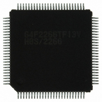
DF2266TF13V Renesas Electronics America, DF2266TF13V Datasheet - Page 595

DF2266TF13V
Manufacturer Part Number
DF2266TF13V
Description
IC H8S/2266 MCU FLASH 100-TQFP
Manufacturer
Renesas Electronics America
Series
H8® H8S/2200r
Datasheet
1.DF2266TF20V.pdf
(712 pages)
Specifications of DF2266TF13V
Core Processor
H8S/2000
Core Size
16-Bit
Speed
13MHz
Connectivity
I²C, SCI, SmartCard
Peripherals
LCD, POR, PWM, WDT
Number Of I /o
67
Program Memory Size
128KB (128K x 8)
Program Memory Type
FLASH
Ram Size
8K x 8
Voltage - Supply (vcc/vdd)
3 V ~ 5.5 V
Data Converters
A/D 10x10b
Oscillator Type
Internal
Operating Temperature
-20°C ~ 75°C
Package / Case
100-TQFP, 100-VQFP
Lead Free Status / RoHS Status
Lead free / RoHS Compliant
Eeprom Size
-
- Current page: 595 of 712
- Download datasheet (5Mb)
Note: * When watch mode or subactive mode is entered, set high-speed mode.
21.2
System clock pulses can be supplied by connecting a crystal resonator, or by input of an external
clock.
21.2.1
A crystal resonator can be connected as shown in the example in figure 21.2. Select the damping
resistance R
Bit
1
0
System Clock Oscillator
Connecting a Crystal Resonator
Bit Name
STC1
STC0
d
according to table 21.1. An AT-cut parallel-resonance crystal should be used.
Note: C
Figure 21.2 Connection of Crystal Resonator (Example)
Initial
Value
0
0
L1
and C
EXTAL
XTAL
L2
are reference values including the floating capacitance of the board.
R/W
R/W
R/W
R
d
Description
Multiplication factor setting
Specifies multiplication factor of the PLL circuit built in the
evaluation chip. The specified multiplication factor
becomes valid software standby mode, watch mode, or
subactive mode is entered.
These bits should be set to 11 in this LSI. Since the value
becomes STC1 = STC0 = 0 after a reset, set STC1 =
STC0 = 1.
00: × 1
01: × 2 (setting prohibited)
10: × 4 (setting prohibited)
11: PLL is bypass
C
C
L1
L2
Rev. 5.00 Sep. 01, 2009 Page 543 of 656
C
L1
Section 21 Clock Pulse Generator
= C
L2
= 10 to 22 pF
REJ09B0071-0500
Related parts for DF2266TF13V
Image
Part Number
Description
Manufacturer
Datasheet
Request
R

Part Number:
Description:
CONN SOCKET 2POS 7.92MM WHITE
Manufacturer:
Hirose Electric Co Ltd
Datasheet:

Part Number:
Description:
CONN SOCKET 4POS 7.92MM WHITE
Manufacturer:
Hirose Electric Co Ltd
Datasheet:

Part Number:
Description:
CONN SOCKET 5POS 7.92MM WHITE
Manufacturer:
Hirose Electric Co Ltd
Datasheet:

Part Number:
Description:
CONN SOCKET 3POS 7.92MM WHITE
Manufacturer:
Hirose Electric Co Ltd
Datasheet:

Part Number:
Description:
CONN SOCKET 5POS 7.92MM WHITE
Manufacturer:
Hirose Electric Co Ltd
Datasheet:

Part Number:
Description:
CONN SOCKET 2POS 7.92MM WHITE
Manufacturer:
Hirose Electric Co Ltd
Datasheet:

Part Number:
Description:
CONN SOCKET 3POS 7.92MM WHITE
Manufacturer:
Hirose Electric Co Ltd
Datasheet:

Part Number:
Description:
CONN SOCKET 4POS 7.92MM WHITE
Manufacturer:
Hirose Electric Co Ltd
Datasheet:

Part Number:
Description:
CONN HEADER 2POS 7.92MM R/A TIN
Manufacturer:
Hirose Electric Co Ltd
Datasheet:

Part Number:
Description:
CONN HEADER 4POS 7.92MM R/A TIN
Manufacturer:
Hirose Electric Co Ltd
Datasheet:

Part Number:
Description:
KIT STARTER FOR M16C/29
Manufacturer:
Renesas Electronics America
Datasheet:

Part Number:
Description:
KIT STARTER FOR R8C/2D
Manufacturer:
Renesas Electronics America
Datasheet:

Part Number:
Description:
R0K33062P STARTER KIT
Manufacturer:
Renesas Electronics America
Datasheet:

Part Number:
Description:
KIT STARTER FOR R8C/23 E8A
Manufacturer:
Renesas Electronics America
Datasheet:

Part Number:
Description:
KIT STARTER FOR R8C/25
Manufacturer:
Renesas Electronics America
Datasheet:


