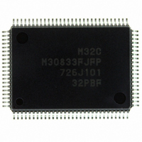
M30833FJFP#U5 Renesas Electronics America, M30833FJFP#U5 Datasheet - Page 232

M30833FJFP#U5
Manufacturer Part Number
M30833FJFP#U5
Description
IC M32C/83 MCU FLASH 100QFP
Manufacturer
Renesas Electronics America
Series
M16C™ M32C/80r
Datasheets
1.M3087BFLGPU3.pdf
(364 pages)
2.M30833FJGPU3.pdf
(96 pages)
3.M30833FJGPU3.pdf
(529 pages)
Specifications of M30833FJFP#U5
Core Processor
M32C/80
Core Size
16/32-Bit
Speed
32MHz
Connectivity
CAN, I²C, IEBus, SIO, UART/USART
Peripherals
DMA, WDT
Number Of I /o
85
Program Memory Size
512KB (512K x 8)
Program Memory Type
FLASH
Ram Size
31K x 8
Voltage - Supply (vcc/vdd)
3 V ~ 5.5 V
Data Converters
A/D 26x10b; D/A 2x8b
Oscillator Type
Internal
Operating Temperature
-20°C ~ 85°C
Package / Case
100-QFP
For Use With
R0K330879S001BE - KIT DEV RSK M32C/87R0K330879S000BE - KIT DEV RSK M32C/87
Lead Free Status / RoHS Status
Lead free / RoHS Compliant
Eeprom Size
-
Available stocks
Company
Part Number
Manufacturer
Quantity
Price
Part Number:
M30833FJFP#U5M30833FJFP#U3
Manufacturer:
Renesas Electronics America
Quantity:
135
Part Number:
M30833FJFP#U5M30833FJFP#U3
Manufacturer:
Renesas Electronics America
Quantity:
10 000
- Current page: 232 of 529
- Download datasheet (5Mb)
R
R
M
e
E
3
. v
J
Figure 16.23 Serial Bus Communication Control with SS Pin
2
0
16.4.1 SSi Input Pin Function (i=0 to 4)
1
9
C
3 .
B
8 /
When the SSE bit in the UiSMR3 register is set to "1" (SS function enabled), the SSi input pin function is
selected, activating the pin function.
The DINC bit in the UiSMR3 register determines which microcomputer performs as master or slave.
When multiple microcomputers perform as the masters (multi-master system), the SSi pin setting deter-
mines which master microcomputer is active and when.
0
1
16.4.1.1 When Setting the DINC Bit to "1" (Slave Mode)
16.4.1.2 When Setting the DINC Bit to "0" (Master Mode)
3
0
3
When an "H" signal is applied to the SSi pin, the STxDi and SRxDi pins are placed in a high-imped-
ance state and the transfer clock input to the CLKi pin is ignored. When a low-level signal ("L") is
applied to the SSi input pin, the transfer clock input is valid and serial communication is enabled.
When an "H" signal is applied to the SSi pin, serial communication is available due to transmission
privilege. The master outputs the transfer clock. When an "L" signal is applied to the SSi pin, it indi-
cates that another master is active and TxDi, RxDi and CLKi pins are placed in a high-impedance
state. Moreover, a fault error occurs and the IR bit in the BCNiIC register is set to "1" (interrupt
requested). The ERR bit in the UiSMR3 register indicates whether a fault error occurs.
In master mode, software interrupt numbers 39, 40 and 41 are used for the fault error interrupt. The
fault error interrupt is generated when the ERR bit changes "0" to "1". The fault error interrupt of
UART0 and of UART3 share an interrupt vector. The fault error interrupt of UART1 and of UART4
share an interrupt vector. The IFSR6 and IFSR7 bits in the IFSR register determine which fault error
interrupt is used.
Communication is not terminated even if a fault error is generated while communicating. To stop
communication, the SMD 2 to SMD0 bit in the UiMR register is set to "000
J
G
4
a
0 -
n
o r
3 .
______
1
u
, 1
3
p
1
2
(
M
0
0
3
6
2
C
Page 207
8 /
_____
, 3
M
3
2
C
f o
Microcomputer
8 /
4
Master
3
8
P9
) T
P9
P9
8
P9
1(
0(
2(
3(
RxD
CLK
TxD
SS
P1
P1
3
3
3
3
3
2
)
)
)
)
_____
_____
____
___
P9
P9
P9
P9
P9
P9
P9
P9
3(
0(
2(
3(
0(
2(
Microcomputer
1(
1(
Microcomputer
SS
CLK
SRxD
SS
CLK
SRxD
STxD
STxD
3
3
Slave
Slave
)
)
3
3
)
)
3
3
3
3
)
)
)
)
16. Serial I/O (Special Function)
2
" (serial I/O disabled).
______
______
_____
Related parts for M30833FJFP#U5
Image
Part Number
Description
Manufacturer
Datasheet
Request
R

Part Number:
Description:
KIT STARTER FOR M16C/29
Manufacturer:
Renesas Electronics America
Datasheet:

Part Number:
Description:
KIT STARTER FOR R8C/2D
Manufacturer:
Renesas Electronics America
Datasheet:

Part Number:
Description:
R0K33062P STARTER KIT
Manufacturer:
Renesas Electronics America
Datasheet:

Part Number:
Description:
KIT STARTER FOR R8C/23 E8A
Manufacturer:
Renesas Electronics America
Datasheet:

Part Number:
Description:
KIT STARTER FOR R8C/25
Manufacturer:
Renesas Electronics America
Datasheet:

Part Number:
Description:
KIT STARTER H8S2456 SHARPE DSPLY
Manufacturer:
Renesas Electronics America
Datasheet:

Part Number:
Description:
KIT STARTER FOR R8C38C
Manufacturer:
Renesas Electronics America
Datasheet:

Part Number:
Description:
KIT STARTER FOR R8C35C
Manufacturer:
Renesas Electronics America
Datasheet:

Part Number:
Description:
KIT STARTER FOR R8CL3AC+LCD APPS
Manufacturer:
Renesas Electronics America
Datasheet:

Part Number:
Description:
KIT STARTER FOR RX610
Manufacturer:
Renesas Electronics America
Datasheet:

Part Number:
Description:
KIT STARTER FOR R32C/118
Manufacturer:
Renesas Electronics America
Datasheet:

Part Number:
Description:
KIT DEV RSK-R8C/26-29
Manufacturer:
Renesas Electronics America
Datasheet:

Part Number:
Description:
KIT STARTER FOR SH7124
Manufacturer:
Renesas Electronics America
Datasheet:

Part Number:
Description:
KIT STARTER FOR H8SX/1622
Manufacturer:
Renesas Electronics America
Datasheet:

Part Number:
Description:
KIT DEV FOR SH7203
Manufacturer:
Renesas Electronics America
Datasheet:


