M30833FJFP#U5 Renesas Electronics America, M30833FJFP#U5 Datasheet - Page 433
M30833FJFP#U5
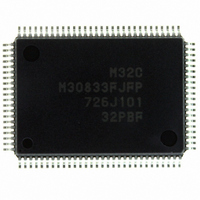
Manufacturer Part Number
M30833FJFP#U5
Description
IC M32C/83 MCU FLASH 100QFP
Manufacturer
Renesas Electronics America
Series
M16C™ M32C/80r
Datasheets
1.M3087BFLGPU3.pdf
(364 pages)
2.M30833FJGPU3.pdf
(96 pages)
3.M30833FJGPU3.pdf
(529 pages)
Specifications of M30833FJFP#U5
Core Processor
M32C/80
Core Size
16/32-Bit
Speed
32MHz
Connectivity
CAN, I²C, IEBus, SIO, UART/USART
Peripherals
DMA, WDT
Number Of I /o
85
Program Memory Size
512KB (512K x 8)
Program Memory Type
FLASH
Ram Size
31K x 8
Voltage - Supply (vcc/vdd)
3 V ~ 5.5 V
Data Converters
A/D 26x10b; D/A 2x8b
Oscillator Type
Internal
Operating Temperature
-20°C ~ 85°C
Package / Case
100-QFP
For Use With
R0K330879S001BE - KIT DEV RSK M32C/87R0K330879S000BE - KIT DEV RSK M32C/87
Lead Free Status / RoHS Status
Lead free / RoHS Compliant
Eeprom Size
-
Available stocks
Company
Part Number
Manufacturer
Quantity
Price

Part Number:
M30833FJFP#U5M30833FJFP#U3
Manufacturer:
Renesas Electronics America
Quantity:
135
Part Number:
M30833FJFP#U5M30833FJFP#U3
Manufacturer:
Renesas Electronics America
Quantity:
10 000


R
R
M
e
E
3
. v
J
2
0
1
9
C
25.3.7 Precautions in CPU Rewrite Mode
3 .
B
8 /
0
1
3
25.3.7.1 Operating Speed
25.3.7.2 Prohibited Instructions
25.3.7.3 Interrupts
25.3.7.4 Reading and Writing Commands and Data
25.3.7.5 Reset
25.3.7.6 Access Prohibited
25.3.7.7 How to Access
25.3.7.8 Rewriting in the User ROM Area
0
3
J
G
Set the MCD register to the following CPU clock before entering CPU rewrite mode .
When the PM12 bit in the PM register is set to "0" (no wait state), 6.25MHz or less
When the PM12 bit in the PM register is set to "1" (wait state), 12.5MHz or less
In CPU rewrite mode, programs cannot be executed, nor can interrupt vectors be read in the flash
memory. Execute the rewrite control program after the program is transferred to a space other than
the flash memory. (See Figure 25.5.)
The following instructions cannot be used because the CPU tries to read data in the flash memory: the
UND instruction, INTO instruction, JMPS instruction, JSRS instruction and BRK instruction.
Read or write 16-bit commands and data from or to even addresses in the user ROM area.
Reset is always enabled.
Write the FMR01 bit and FMR05 bit in a space other than the flash memory.
To set the FMR01 bit and FMR02 bits to "1", set to "1" immediately after setting to "0". Do not generate
an interrupt or a DMA transfer between the instruction to set the bits to "1" and the instruction to set the
bits to "0". Set the FMR01 bit to "1" after an "H" signal is applied to the P8
If the supply voltage drops while in CPU rewrite mode, when rewriting the block where the rewrite
control program is stored, the flash memory cannot be rewritten because the rewrite control program
is not correctly rewritten. If this error occurs, rewrite the user ROM area while in standard serial I/O
mode or parallel I/O mode.
• To use interrupts having vectors in a relocatable vector table, the vectors must be relocated to the
• The NMI and watchdog timer interrupts are available since the FMR01 is forcibly reset when either
• The address match interrupt is not available since the CPU tries to read data in the flash memory.
4
a
0 -
n
o r
RAM area.
interrupt occurs. Allocate the jump addresses for each interrupt service routine and write to the fixed
vector table. Flash memory rewrite operation is aborted when the NMI or watchdog timer interrupt
occurs. Execute the rewrite program again after exiting the interrupt routine.
3 .
1
u
, 1
3
p
1
_______
2
(
M
0
0
3
6
2
C
8 /
Page 408
, 3
M
3
2
C
f o
8 /
4
3
8
) T
8
_______
5
/NMI pin.
______
25. Flash Memory Version
Related parts for M30833FJFP#U5
Image
Part Number
Description
Manufacturer
Datasheet
Request
R

Part Number:
Description:
KIT STARTER FOR M16C/29
Manufacturer:
Renesas Electronics America
Datasheet:

Part Number:
Description:
KIT STARTER FOR R8C/2D
Manufacturer:
Renesas Electronics America
Datasheet:

Part Number:
Description:
R0K33062P STARTER KIT
Manufacturer:
Renesas Electronics America
Datasheet:

Part Number:
Description:
KIT STARTER FOR R8C/23 E8A
Manufacturer:
Renesas Electronics America
Datasheet:

Part Number:
Description:
KIT STARTER FOR R8C/25
Manufacturer:
Renesas Electronics America
Datasheet:

Part Number:
Description:
KIT STARTER H8S2456 SHARPE DSPLY
Manufacturer:
Renesas Electronics America
Datasheet:

Part Number:
Description:
KIT STARTER FOR R8C38C
Manufacturer:
Renesas Electronics America
Datasheet:

Part Number:
Description:
KIT STARTER FOR R8C35C
Manufacturer:
Renesas Electronics America
Datasheet:

Part Number:
Description:
KIT STARTER FOR R8CL3AC+LCD APPS
Manufacturer:
Renesas Electronics America
Datasheet:
Part Number:
Description:
KIT STARTER FOR RX610
Manufacturer:
Renesas Electronics America
Datasheet:

Part Number:
Description:
KIT STARTER FOR R32C/118
Manufacturer:
Renesas Electronics America
Datasheet:

Part Number:
Description:
KIT DEV RSK-R8C/26-29
Manufacturer:
Renesas Electronics America
Datasheet:

Part Number:
Description:
KIT STARTER FOR SH7124
Manufacturer:
Renesas Electronics America
Datasheet:

Part Number:
Description:
KIT STARTER FOR H8SX/1622
Manufacturer:
Renesas Electronics America
Datasheet:

Part Number:
Description:
KIT DEV FOR SH7203
Manufacturer:
Renesas Electronics America
Datasheet: